
Substrate for power module and manufacturing method therefor

A technology of power modules and manufacturing methods, which is applied in the directions of manufacturing tools, printed circuit manufacturing, chemical instruments and methods, etc., can solve problems such as peeling of ceramic substrates and metal plates, prevent peeling, improve bonding reliability, and reduce anisotropy Effect

Active Publication Date: 2014-11-26
MITSUBISHI MATERIALS CORP
View PDF7 Cites 0 Cited by
  • Summary
  • Abstract
  • Description
  • Claims
  • Application Information

AI Technical Summary

Problems solved by technology

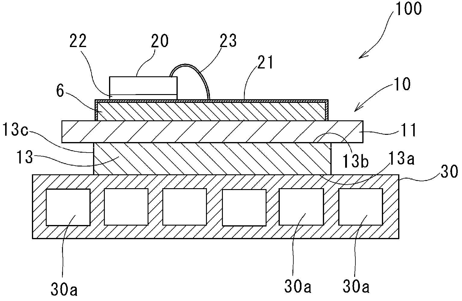
[0009] In such a substrate for a power module, microscopic voids sometimes occur at the solder joint between the ceramic substrate and the metal plate. Delamination occurs at the joint interface with the metal plate

Method used


Image

  • Substrate for power module and manufacturing method therefor
  • Substrate for power module and manufacturing method therefor
  • Substrate for power module and manufacturing method therefor

Examples


Embodiment

[0062] In order to confirm the effects of the present invention, the following experiments were conducted.

[0063] A rolled material made of 1N99 aluminum with a thickness of 0.6 mm was punched out into 30 mm×30 mm, etched or blasted as shown in Table 1, and the removal depth of the metal plate surface by this treatment was measured. The removal amount was calculated from the difference between the weight before treatment and the weight after treatment of the metal plate, and the removal depth was obtained from the relationship between the removal amount and the specific gravity and area of ​​the metal plate.

[0064] Also, for the metal plate with the treated surface, the oxygen concentration is analyzed by the number of oxygen meters measured with an electron probe microanalyzer (EPMA) at an accelerating voltage of 10kV, a current of 100mA, and a beam diameter of 100μm, and X-rays in the thickness direction Photoelectron spectroscopy (XPS) was used to determine the oxide th...


PUM

PropertyMeasurementUnit
thicknessaaaaaaaaaa
lengthaaaaaaaaaa
mean roughnessaaaaaaaaaa

Abstract

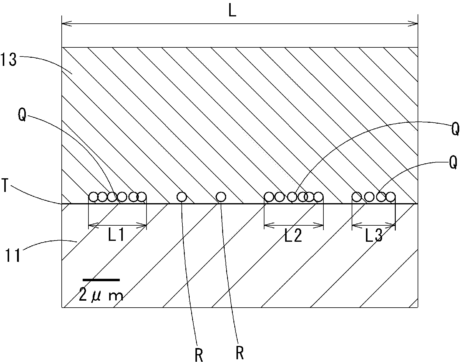
Provided is a substrate for a power module, that reduces micro voids in join sections and prevents detachment, and a manufacturing method therefor. In the present invention, a metal plate made of aluminum or an aluminum alloy is joined to at least one face of a ceramic substrate by brazing. When a cross-section of the metal plate within a region 200µm wide from the side edge of the metal plate and within a depth of 5µm from the joining interface between the metal plate and the ceramic substrate is observed at 3000x magnification with a scanning electron microscope, the total length of consecutive residual oxide that is present consecutively for 2µm or more along the joining interface is 70% or less relative to the viewing length.

Description

technical field [0001] The present invention relates to a substrate for a power module constituting a power module controlling a large current and a high voltage, and a manufacturing method thereof. [0002] This application claims priority based on Patent Application No. 2012-077401 for which it applied in Japan on March 29, 2012, and uses the content here. Background technique [0003] Conventionally, as a semiconductor device that controls a large current and a high voltage, a power module having a structure in which electronic components such as a semiconductor chip are mounted on a power module substrate is known. As a method of manufacturing a power module, methods described in Patent Document 1 and Patent Document 2 are known, for example. In these manufacturing methods, first, a metal plate to be a circuit layer is laminated on one side of a ceramic substrate with a solder, and a metal plate to be a heat dissipation layer is laminated on the other side of a ceramic ...

Claims


Application Information

Patent Timeline
Patent Type & Authority Applications(China)
IPC IPC(8): H01L23/13H05K1/02
CPCC04B2235/6581C04B2237/52H01L2224/73265C04B2237/366C04B2237/704C04B2237/126C04B2235/963C04B37/026H01L23/473H01L2224/48091C04B2237/708C04B2237/86C04B2237/402H01L23/3735C04B2237/706C04B2237/60C04B2237/128H01L23/3736C04B2237/121B32B18/00H05K3/382H05K3/383C04B2235/723H05K1/0306C04B2237/064C04B2237/592C04B2237/72H01L2924/00014B23K1/0016B32B15/04B23K1/19B32B2457/00
Inventor 长濑敏之北原丈嗣村中亮
Owner MITSUBISHI MATERIALS CORP
Learn More