Substrate for power module and manufacturing method thereof
A technology for power modules and manufacturing methods, applied in manufacturing tools, printed circuit manufacturing, chemical instruments and methods, etc., can solve problems such as peeling off of ceramic substrates and metal plates, prevent peeling, improve bonding reliability, and reduce anisotropy Effect
- Summary
- Abstract
- Description
- Claims
- Application Information
AI Technical Summary
Problems solved by technology
Method used
Image

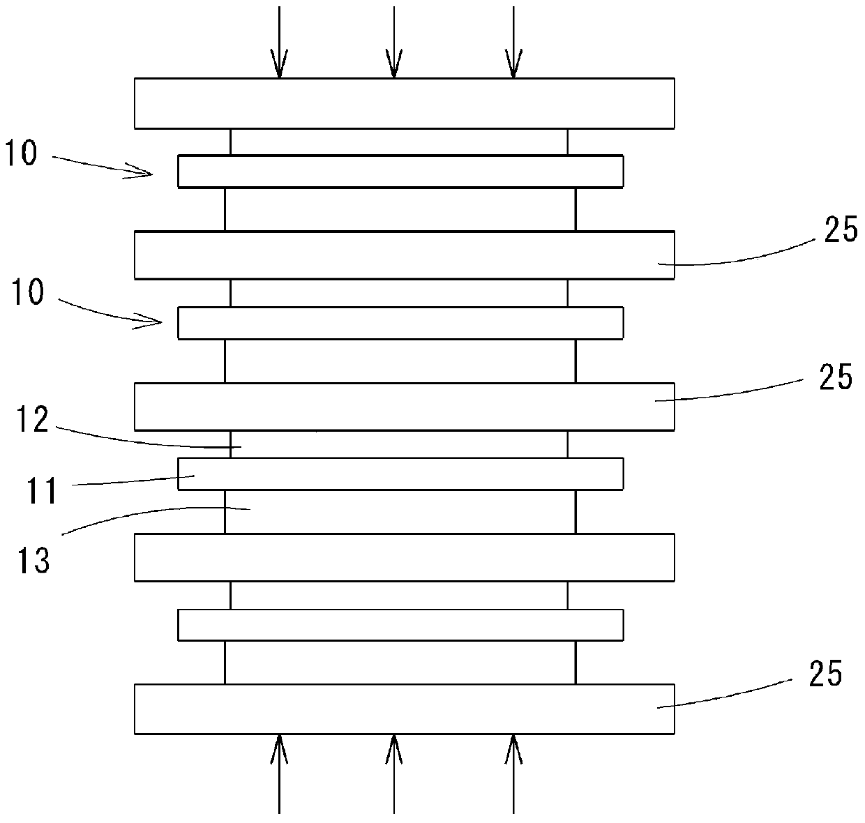
Examples
Embodiment
[0062] In order to confirm the effects of the present invention, the following experiments were conducted.
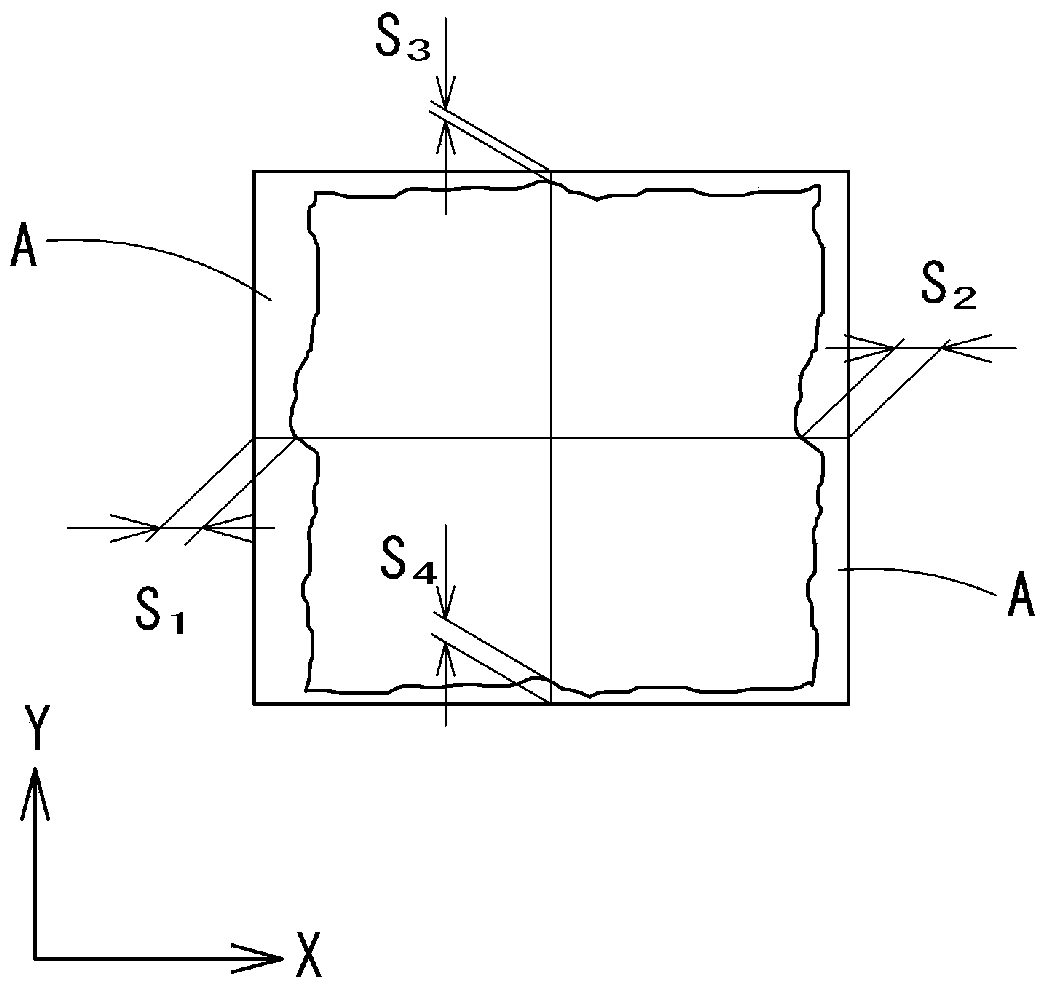
[0063] A rolled material made of 1N99 aluminum with a thickness of 0.6 mm was punched out into 30 mm×30 mm, etched or blasted as shown in Table 1, and the removal depth of the metal plate surface by this treatment was measured. The removal amount was calculated from the difference between the weight before treatment and the weight after treatment of the metal plate, and the removal depth was obtained from the relationship between the removal amount and the specific gravity and area of the metal plate.
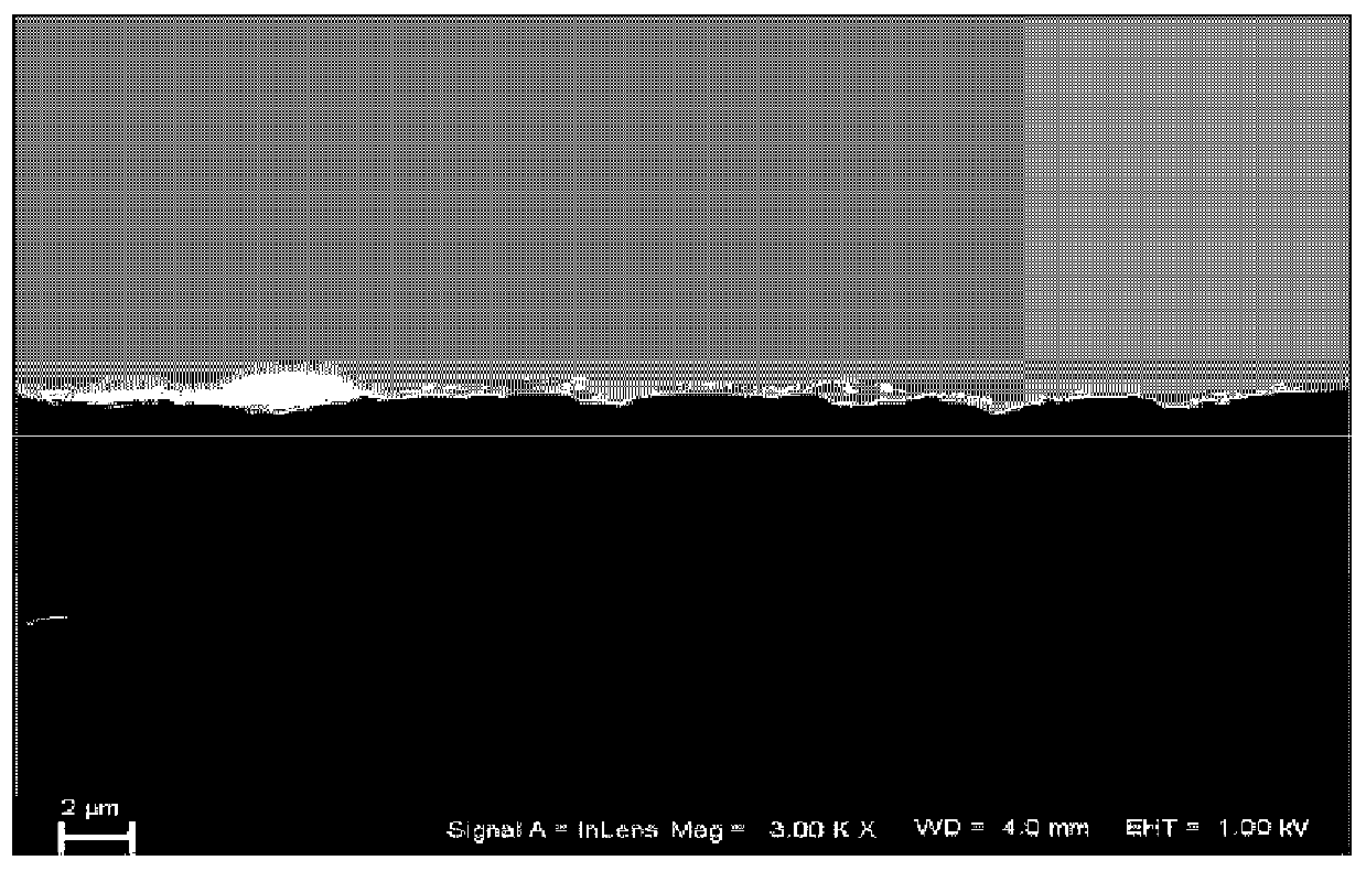
[0064] Also, for the metal plate with the treated surface, the oxygen concentration is analyzed by the number of oxygen meters measured with an electron probe microanalyzer (EPMA) at an accelerating voltage of 10kV, a current of 100mA, and a beam diameter of 100μm, and X-rays in the thickness direction Photoelectron spectroscopy (XPS) was used to determine the oxide th...
PUM
| Property | Measurement | Unit |
|---|---|---|
| thickness | aaaaa | aaaaa |
| length | aaaaa | aaaaa |
| mean roughness | aaaaa | aaaaa |
Abstract
Description
Claims
Application Information