Method for manufacturing nanometer laser device arrays

A technology of nano-laser and manufacturing method, which is applied in the field of optics, can solve the problems of adding nano-laser components, inability to realize flexible manipulation of lasers, and difficulty in nano-laser arrays, so as to achieve difficult manufacturing process, poor flexibility in array distribution, and reliable performance sex high effect

Inactive Publication Date: 2014-12-17
HANGZHOU DIANZI UNIV
View PDF4 Cites 3 Cited by
  • Summary
  • Abstract
  • Description
  • Claims
  • Application Information

AI Technical Summary

Problems solved by technology

Although this prior art has certain advantages, there are essential deficiencies: First, the use of coaxial multi-layer cylindrical shell structure has a complex structure, and there are many parameters with high precision requirements on the micro-nano structure, and the parameter values ​​are diverse, resulting in The manufacturing process is difficult and the maneuverability is inflexible; secondly, the nano-laser structure needs the substrate as a support, increasing the components of the nano-laser increases the size of the device as a whole, and the laser structure and the substrate are fixed to each other, so the laser cannot be flexibly manipulated; and, It is very difficult to realize nano-laser array, and the flexibility of array distribution is poor

Method used


Image

  • Method for manufacturing nanometer laser device arrays
  • Method for manufacturing nanometer laser device arrays
  • Method for manufacturing nanometer laser device arrays

Examples


Embodiment Construction

[0025] The present invention will be further described below in conjunction with drawings and embodiments.

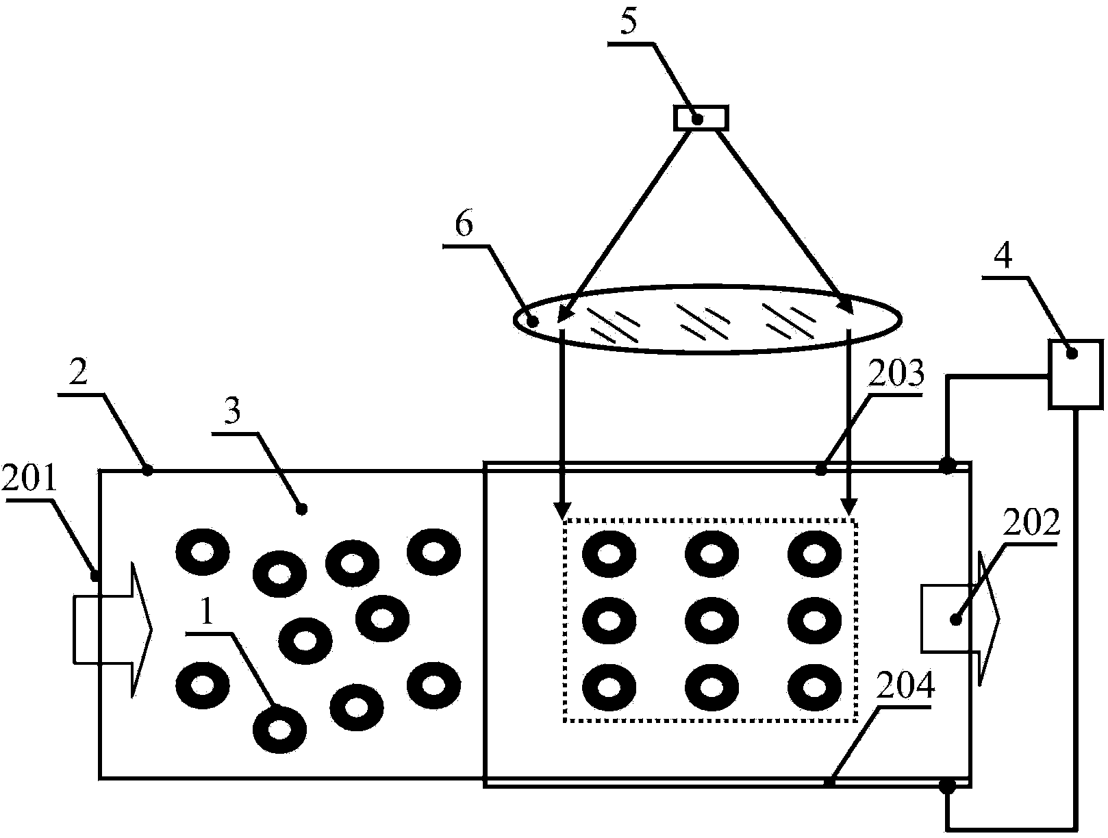
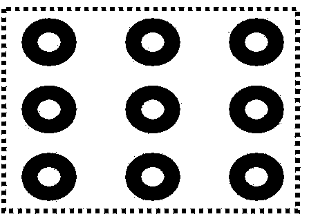
[0026] The present invention is based on the interaction mechanism of multilayer spherical shell nano optics and plasma modes, adopts multilayer spherical shell nano lasers, combines electrorheological effects to arrange and solidify the nano lasers, obtains nano laser arrays, and provides a nano laser Array production method, the specific production steps are as follows:

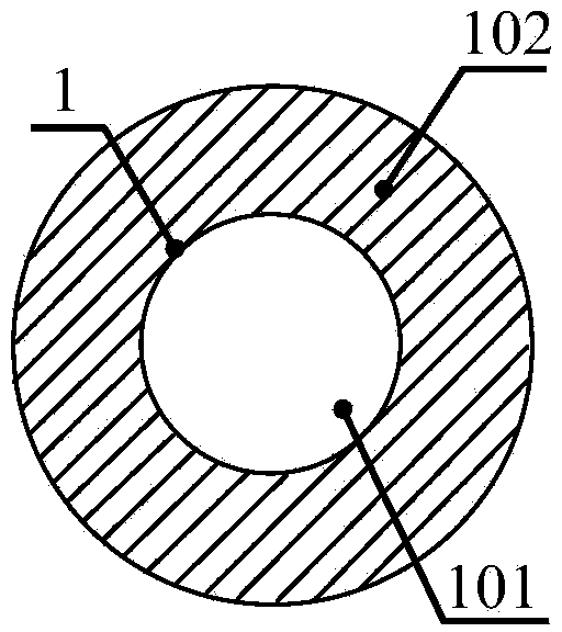
[0027] Step (1) Dispersing the nano-laser 1 into the photocurable glue fluid 3 to form a nano-laser suspension, a single nano-laser adopts a spherical shell structure, including a metal sphere core 101 and a non-metallic outer spherical shell 102 doped with dye molecules, And the radius of the metal sphere core 101 is less than 100 nanometers, and the number of dye molecules contained in the non-metal outer spherical shell 102 is greater than 2000;

[0028] In this embodiment, the nano-laser consist...


PUM


Abstract

The invention relates to a method for manufacturing nanometer laser device arrays. By the aid of the method, problems of complicated process and low flexibility and controllability in the prior art can be solved. The method is based on multilayer spherical shell nanometer optical and plasma mode interaction mechanisms, and multilayer spherical shell laser devices are combined with electrorheological effects to be arrayed and are solidified to obtain the nanometer laser device arrays. The method has the advantages that the laser devices are simple in structure, a manufacturing process is simple, fixing substrates for the structures of the nanometer laser devices can be omitted, the method for manufacturing the nanometer laser device arrays is simple and is high in controllability, the arrays can be flexibly distributed, the shapes of the integral devices can be flexibly selected, and the like.

Description

technical field [0001] The invention belongs to the field of optical technology, and relates to a method for manufacturing a laser, in particular to a method for manufacturing a nanometer laser array. It is mainly used in micro-opto-electromechanical, optoelectronic integration, photoelectric detection, optical communication, optical information storage, optical microscopy, lithography, super-resolution and other fields. technical background [0002] A laser is a device that uses the principle of stimulated radiation to amplify or oscillate light in certain excited substances. A laser usually includes: an excitation source, a working medium, and a resonator. The excitation is that the working medium absorbs external energy and is excited to an excited state, creating conditions for realizing and maintaining particle population inversion; the working medium has a metastable energy level to make the stimulated radiation occupy Dominance, thereby achieving optical amplificatio...

Claims


Application Information

Patent Timeline
IPC IPC(8): H01S5/022H01S5/40B82Y20/00
Inventor 高秀敏张艳林李楠南学芳郁敏
Owner HANGZHOU DIANZI UNIV
Why Eureka
Try Eureka