

High-voltage electrostatic discharge(ESD) protection circuit for stacked substrate-trigger silicon controlled rectier (STSCR) and laterally diffused metal oxide semiconductors (LDMOSs)
A high-voltage, circuit technology, applied in the field of electronics, can solve the problems of burnt-out devices, low maintenance voltage, etc., and achieve the effect of reducing the risk of latch-up effect
- Summary
- Abstract
- Description
- Claims
- Application Information
AI Technical Summary
Problems solved by technology
Method used
Image

Examples
Embodiment 1
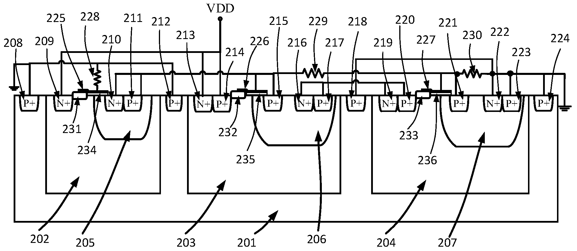
[0038] image 3 The structural schematic diagram of the high-voltage ESD protection circuit of the LDMOS trigger stack STSCR-LDMOS provided in this embodiment includes a P-type substrate 201, a first high-voltage N-type well region 202, a second high-voltage N-type well region 203, and a third high-voltage N-type well region. type well region 204, the first P type well region 205, the second P type well region 206, the third P type well region 207, the first P type heavily doped region 208, the second P type heavily doped region 211, the second P type well region Three P-type heavily doped regions 212, fourth P-type heavily doped regions 214, fifth P-type heavily doped regions 215, sixth P-type heavily doped regions 217, seventh P-type heavily doped regions 218, Eight P-type heavily doped regions 220, ninth P-type heavily doped regions 221, tenth P-type heavily doped regions 223, eleventh P-type heavily doped regions 224, first N-type heavily doped regions 209, The second N-t...
Embodiment 2
[0052] Such as Figure 5 As shown, this embodiment uses PLDMOS instead of NLDMOS on the basis of Embodiment 1. At this time, the other end of the resistor 228 connected to the gate of PLDMOS is connected to the anode of STSCR-LDMOS1, and the rest of the connection methods are the same as those of NLDMOS , the working principle of this embodiment is the same as that of Embodiment 1.
[0053] Embodiment 2 uses PLDMOS instead of NLDMOS to trigger the stacked STSCR-LDMOS structure, because PLDMOS has a higher sustain voltage than NLDMOS, so that the sustain voltage after the first snapback is higher, so the anti-noise capability is stronger.
Embodiment 3
[0055] Such as Figure 8 As shown, this embodiment removes the resistor 230 on the basis of Embodiment 1. The working principle of this embodiment is the same as that of Embodiment 1.
[0056] In Embodiment 3, the resistor 230 is removed, so that all the current after the breakdown of the NLDMOS flows through the resistor 304, which can increase the turn-on speed of the STSCR-LDMOS.
[0057] Figure 6 The equivalent circuit diagram of the high-voltage ESD protection circuit of the LDMOS trigger stacked STSCR-LDMOS provided by the present invention. The present invention can greatly increase the sustain voltage by stacking more STSCR-LDMOS stacked units 501, and more effectively prevent the occurrence of latch-up effect.
[0058] Figure 7 The I-V curve simulation diagram of NLDMOS triggering different stack numbers of STSCR-LDMOS is given, from Figure 7 It can be seen that, as the number of stacks increases, the breakdown voltage increases from 70V to 74.8V, while the su...
PUM
 Abstract
Description
Claims
Application Information