Metal antenna structure for improving slow axis far field of surface emission semiconductor laser unit

An antenna structure and laser technology, applied in optics, instruments, optical components, etc., can solve the problems of unsuitable mass production, difficult process, high price, etc. High precision engraving

Active Publication Date: 2015-01-07
INST OF SEMICONDUCTORS - CHINESE ACAD OF SCI
View PDF5 Cites 6 Cited by
  • Summary
  • Abstract
  • Description
  • Claims
  • Application Information

AI Technical Summary

Problems solved by technology

However, since focused ion beam etching (FIB) technology is required to make metal patterns on the laser cavity surface, the process is difficult and extremely expensive, and it is not suitable for large-scale batch production

Method used


Image

  • Metal antenna structure for improving slow axis far field of surface emission semiconductor laser unit
  • Metal antenna structure for improving slow axis far field of surface emission semiconductor laser unit

Examples


Embodiment Construction

[0024] In order to make the object, technical solution and advantages of the present invention clearer, the present invention will be described in further detail below in conjunction with specific embodiments and with reference to the accompanying drawings.

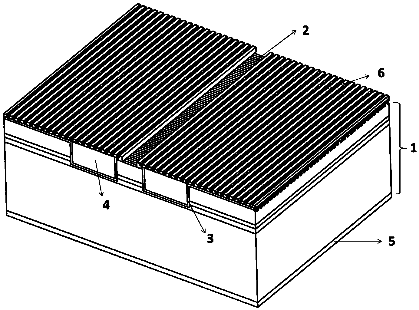
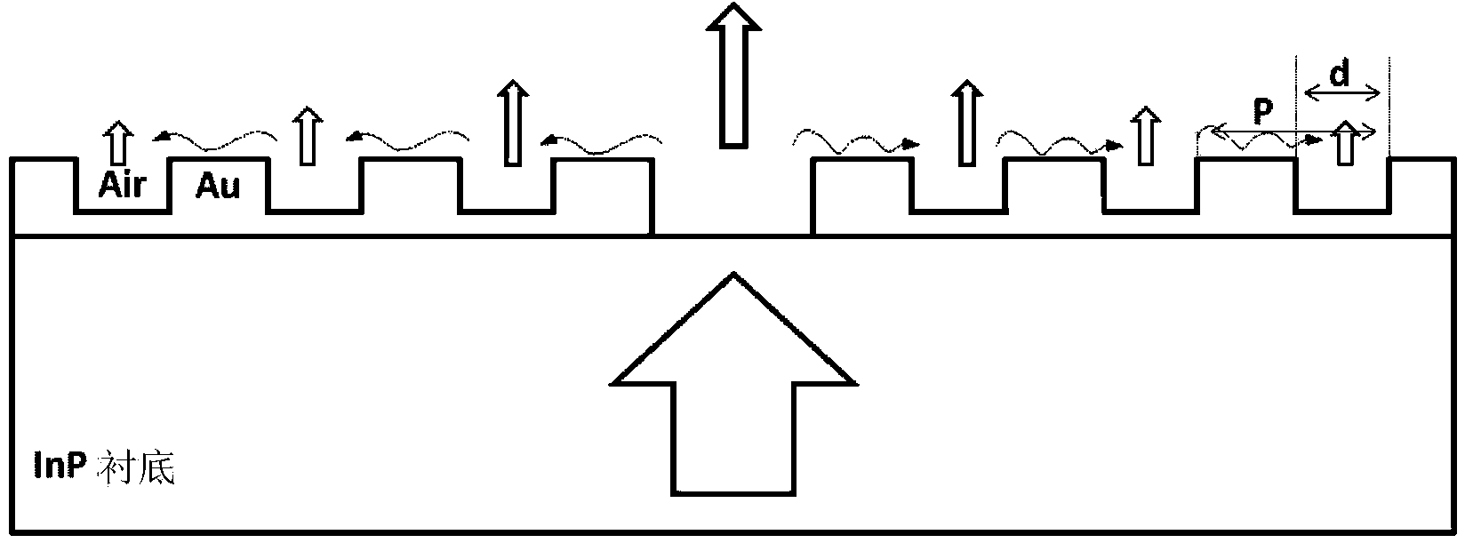
[0025] The invention provides a metal antenna structure for improving the slow axis far field of a surface-emitting semiconductor laser, figure 1 A three-dimensional structure schematic diagram of a metal antenna for improving the slow-axis far field of a surface-emitting semiconductor laser according to an embodiment of the present invention is given. Such as figure 1 As shown, the antenna includes: a substrate 1, a grating layer 2, an electrical isolation layer 3, a double groove filling 4, a lower ohmic contact layer 5, and a subwavelength metal plasma antenna 6, wherein:

[0026] A double-channel ridge waveguide structure is fabricated on the substrate 1, and the ridge area of ​​the double-channel ridge waveguide str...


PUM


Abstract

The invention discloses a metal antenna structure for improving the slow axis far field of a surface emission semiconductor laser unit. The metal antenna structure comprises a substrate, a grating layer, an electrical isolation layer, double-channel filler, a lower ohmic contact layer and a sub-wavelength metal plasma antenna, wherein the substrate is provided with a double-channel ridge-shaped waveguide structure, and a laser unit active region is arranged inside a ridge-shaped region; the grating layer is arranged on the upper surface of the substrate; the electrical isolation layer is arranged on the upper surface of the grating layer, and an electric injection window is formed by breaking the position, corresponding to the ridge-shaped region, on the upper surface of the grating layer; double channels are filled with the double-channel filler; the lower ohmic contact layer is arranged on the lower surface of the substrate; the sub-wavelength metal plasma antenna is arranged on the upper surface of the electrical isolation layer and the upper surface of the double-channel filler, and an electric injection ohmic contact region and a light output window are formed at the same time in the mode that the position, corresponding to the ridge-shaped region, of the sub-wavelength metal plasma antenna is broken. The metal antenna structure effectively reduces the far field divergence angle in the slow axis direction of the surface emission laser unit, and realizes manufacturing of a small-divergence-angle quasi-circular spot or even circular spot surface emission device.

Description

technical field [0001] The invention relates to the field of semiconductor optoelectronic technology, in particular to a metal antenna structure for improving the slow-axis far field of a surface-emitting semiconductor laser. Background technique [0002] Far field is an important index of semiconductor laser. Surface-emitting semiconductor lasers using two-stage Bragg distributed feedback gratings are widely used in atmospheric environment monitoring, optical fiber communications, and free Space optical communication transmitter system. However, due to the device configuration, the far field of the surface emitting semiconductor laser is not perfect, and the far field in the ridge width direction (slow axis) maintains a large divergence angle, usually between 10° and 30°. The far-field cross-section of the surface-emitting semiconductor laser presents a long and narrow single-lobed or double-lobed jujube-shaped outline, and there is still a certain gap between the far-fie...

Claims


Application Information

Patent Timeline
Patent Type & Authority Applications(China)
IPC IPC(8): G02B27/09
CPCG02B27/0916
Inventor 姚丹阳张锦川周予虹贾志伟闫方亮王利军刘俊岐刘峰奇王占国
Owner INST OF SEMICONDUCTORS - CHINESE ACAD OF SCI
Why Eureka
Try Eureka