A kind of laser and its manufacturing method

A manufacturing method and laser technology, applied in the field of lasers, can solve problems such as reducing carrier transport capacity and laser conversion efficiency

Active Publication Date: 2018-01-30
INST OF SEMICONDUCTORS - CHINESE ACAD OF SCI
View PDF6 Cites 0 Cited by
  • Summary
  • Abstract
  • Description
  • Claims
  • Application Information

AI Technical Summary

Problems solved by technology

Although this method can improve the above contradictory relationship to a certain extent, the problem of injecting carriers needs to overcome a high potential barrier to enter the active region, which greatly reduces the transport capacity of carriers and the conversion efficiency of the laser.

Method used


Image

  • A kind of laser and its manufacturing method

Examples


Embodiment Construction

[0007] In order to make the object, technical solution and advantages of the present invention clearer, the present invention will be further described in detail below in conjunction with specific embodiments and with reference to the accompanying drawings.

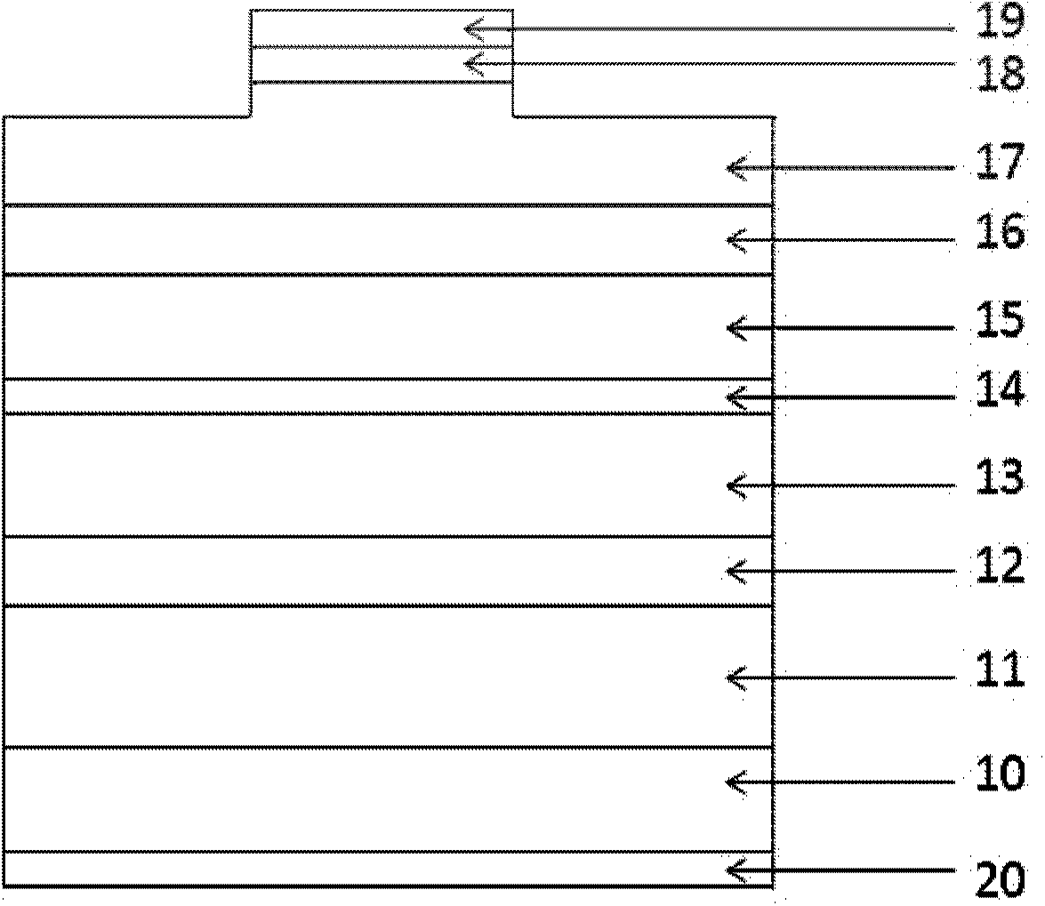
[0008] figure 1 A schematic structural diagram of a laser proposed by the present invention is shown. Such as figure 1 As shown, the laser includes:

[0009] -N-type gallium arsenide substrate 10;

[0010] -N-type cladding layer 11, the N-type cladding layer 11 is fabricated on the N-type gallium arsenide substrate 10;

[0011] - superlattice layer 12, this superlattice layer 12 is made on the N-type cladding layer 11;

[0012] -N-type waveguide layer 13, the N-type waveguide layer 13 is made on the superlattice layer 12;

[0013] - active layer 14, this active layer 14 is made on the N-type waveguide layer 13;

[0014] - P-type waveguide layer 15, the P-type waveguide layer 15 is fabricated on the active layer 14; ...


PUM


Abstract

The invention provides a laser and a manufacturing method thereof. The laser includes: an N-type gallium arsenide substrate; an N-type cladding layer, which is made on the front side of the N-type gallium arsenide substrate; a first superlattice layer, which is made on the N-type cladding layer; an N-type waveguide layer, which is made on the On the superlattice layer; the active layer is made on the N-type waveguide layer; the P-type waveguide layer is made on the active layer; the second superlattice layer is made on the P-type waveguide layer; the P-type cladding layer, Made on the superlattice layer; P-type ohmic contact layer, made on the P-type covering layer; P-type ohmic electrode, made on the P-type ohmic contact layer; N-type ohmic electrode, made on the N-type gallium arsenide substrate (10) BACK. In the present invention, the invention utilizes the superlattice layer to not only provide a low refractive index barrier, but also have a high carrier transport capability, so that the laser has a low threshold current, a low vertical divergence angle and a high carrier transport capability at the same time. luck ability.

Description

technical field [0001] The invention relates to the technical field of semiconductor devices, in particular to a laser with a special structure inserted into a superlattice layer to improve carrier transport and a manufacturing method thereof. Background technique [0002] With the rapid development of semiconductor optoelectronic devices, high-power semiconductor lasers came into being. Due to the advantages of small size, low price, high electro-optical conversion efficiency and long life of semiconductor lasers, semiconductor lasers have a very wide range of applications in the field of optoelectronics. Semiconductor lasers play an important role in the fields of industrial processing, medical treatment, military and theoretical research. Gallium arsenide is the most well-studied material so far compared to other semiconductor III-V materials. Therefore, people have the highest performance requirements for gallium arsenide lasers. This is reflected in the fact that gall...

Claims


Application Information

Patent Timeline
Patent Type & Authority Patents(China)
IPC IPC(8): H01S5/30H01S5/323
Inventor 李翔赵德刚朱建军陈平刘宗顺江德生
Owner INST OF SEMICONDUCTORS - CHINESE ACAD OF SCI
Why Eureka
Try Eureka