Radio frequency transverse double-diffusion field effect transistor and manufacturing method thereof

A field-effect transistor and lateral double-diffusion technology, which is applied in semiconductor/solid-state device manufacturing, semiconductor devices, electrical components, etc., can solve problems that affect the robustness of device hot carrier injection capabilities and affect the service life of devices, and achieve Improved hot carrier injection capability and reduced output capacitance

Active Publication Date: 2015-01-14
SHANGHAI HUAHONG GRACE SEMICON MFG CORP
View PDF5 Cites 5 Cited by
  • Summary
  • Abstract
  • Description
  • Claims
  • Application Information

AI Technical Summary

Problems solved by technology

[0004] In high-frequency applications of RF lateral double-diffused field effect transistors, in order to further reduce the output capacitance (Coss) of the device, the oxide layer under the Faraday shielding metal layer of the R

Method used


Image

  • Radio frequency transverse double-diffusion field effect transistor and manufacturing method thereof
  • Radio frequency transverse double-diffusion field effect transistor and manufacturing method thereof
  • Radio frequency transverse double-diffusion field effect transistor and manufacturing method thereof

Examples


Embodiment 1

[0042] A method for manufacturing a radio-frequency lateral double-diffused field-effect transistor, comprising the following steps:

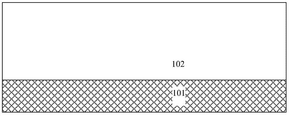
[0043] 1. grow lightly doped P-type epitaxial layer 102 on heavily doped P-type substrate 101, as figure 2 shown;

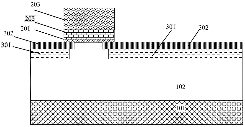
[0044] 2. An oxide layer 201 is thermally oxidized and grown on the P-type epitaxial layer 102, and then a layer of polysilicon 202 is deposited, and the polysilicon gate is photoetched in the middle;

[0045] 3. Keep the photoresist 203 above the polysilicon gate, and perform the first N-type ion implantation 301, the first N-type ion implantation is a self-aligned vertical implantation;

[0046] 4. Keep the photoresist 203 above the polysilicon gate, and perform the second N-type ion implantation 302. The second N-type ion implantation is a self-aligned oblique angle implantation, and the second N-type ion implantation depth is deeper than the first N-type ion implantation. Type ion implantation depth is shallow, such as im...

Embodiment 2

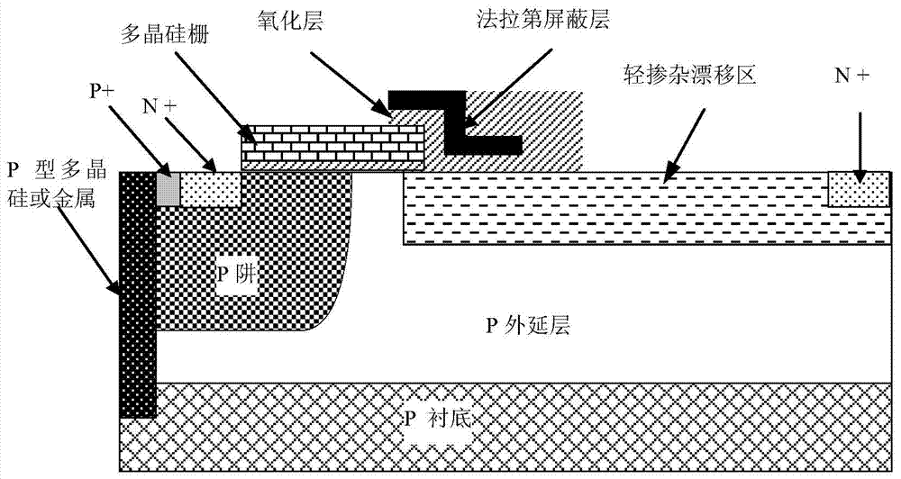
[0063] RF lateral double-diffused field-effect transistors, such as Figure 5 As shown, a P-type epitaxial layer 102 is grown on a P-type substrate 101, and a gate oxide 201 and a polysilicon gate 202 are sequentially formed above the middle of the P-type epitaxial layer 102;

[0064] Form a P well 501 in the P-type epitaxial layer at the lower left of the polysilicon gate 202, and form an N-type drift region in the P-type epitaxial layer at the lower right of the polysilicon gate 202;

[0065] The N-type drift region is divided into a low-depth region, a medium-depth region, and a high-depth region from left to right, the low-depth region is located below the right part of the polysilicon gate, and the high-depth region is a distance away from the right end of the polysilicon gate 202;

[0066] A Faraday shielding oxide layer and a Faraday shielding metal layer are formed on the right part of the polysilicon gate 202 and above the left part of the N-type drift region;

[006...


PUM

PropertyMeasurementUnit
Thicknessaaaaaaaaaa
Thicknessaaaaaaaaaa

Abstract

The invention discloses a radio frequency transverse double-diffusion field effect transistor. A drifting region is of a non-uniform doping structure. The invention further discloses a manufacturing method for the radio frequency transverse double-diffusion field effect transistor. Three times of N-type ion injection is adopted in the drifting region to form a non-uniform N-type structure, self-alignment perpendicular injection of low-dosage medium energy is conducted in the first time of N-type ion injection, self-alignment oblique angle injection of low-dosage low energy is conducted in the second time of N-type ion injection, and then the third time of N-type ion injection is conducted at the position, away from polysilicon gates by a certain distance, in the drifting region through template definition. According to the radio frequency transverse double-diffusion field effect transistor and the manufacturing method thereof, on the condition of a thick Faraday shield oxidation layer, the output capacitance is reduced, the hot carrier injection capability and the robustness are enhanced, and the manufacturing technology is simple.

Description

technical field [0001] The invention relates to semiconductor technology, in particular to a radio-frequency lateral double-diffusion field-effect transistor and a manufacturing method thereof. Background technique [0002] With the advent of the 3G era, more and more communication fields require the development of higher power RF devices. Radio Frequency Lateral Double Diffusion Field Effect Transistor (RFLDMOS), due to its very high output power, has been widely used in portable wireless base station power amplification as early as the 1990s, and its application frequency is 900MHz to 3.8GHz. Compared with traditional silicon-based bipolar transistors, RFLDMOS has better linearity, higher power and gain. Today, RFLDMOS is more popular than bipolar, and GaAs devices. [0003] The current structure of RFLDMOS is as follows Figure 1 As shown, this structure has a lightly doped drift region (LDD) at the drain end, so that it has a larger breakdown voltage (BV), and at the s...

Claims


Application Information

Patent Timeline
IPC IPC(8): H01L29/78H01L21/336
CPCH01L29/0684H01L29/66674H01L29/66681H01L29/7801H01L29/7816
Inventor 李娟娟钱文生
Owner SHANGHAI HUAHONG GRACE SEMICON MFG CORP
Why Eureka
Try Eureka