IGBT (Insulated Gate Bipolar Transistor) and manufacture method thereof

A bipolar transistor and insulated gate technology, applied in semiconductor/solid-state device manufacturing, semiconductor devices, electrical components, etc., can solve problems such as limited application, increased switching loss of devices, and long current tailing of devices

Inactive Publication Date: 2015-01-21
CSMC TECH FAB2 CO LTD
View PDF5 Cites 6 Cited by
  • Summary
  • Abstract
  • Description
  • Claims
  • Application Information

AI Technical Summary

Problems solved by technology

[0004] 1. There is a parasitic thyristor structure inside the device. Under certain conditions, the device is prone to latch-up effect and loses control ability, which reduces the safe working area and causes device failure; therefore, the design and preparation of the PN junction in the IGBT substrate has a great impact on device performance. and reliability performance have a very important impact on
[0005] 2. Due to the conduc

Method used


Image

  • IGBT (Insulated Gate Bipolar Transistor) and manufacture method thereof
  • IGBT (Insulated Gate Bipolar Transistor) and manufacture method thereof
  • IGBT (Insulated Gate Bipolar Transistor) and manufacture method thereof

Examples


Embodiment Construction

[0034] In order to make the purpose, features and advantages of the present invention more comprehensible, specific implementations of the present invention will be described in detail below in conjunction with the accompanying drawings.

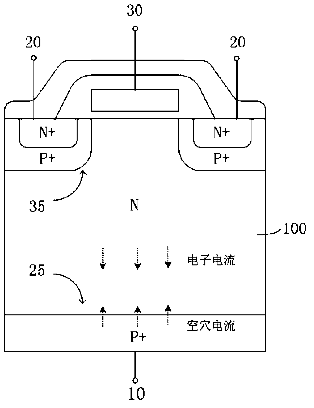
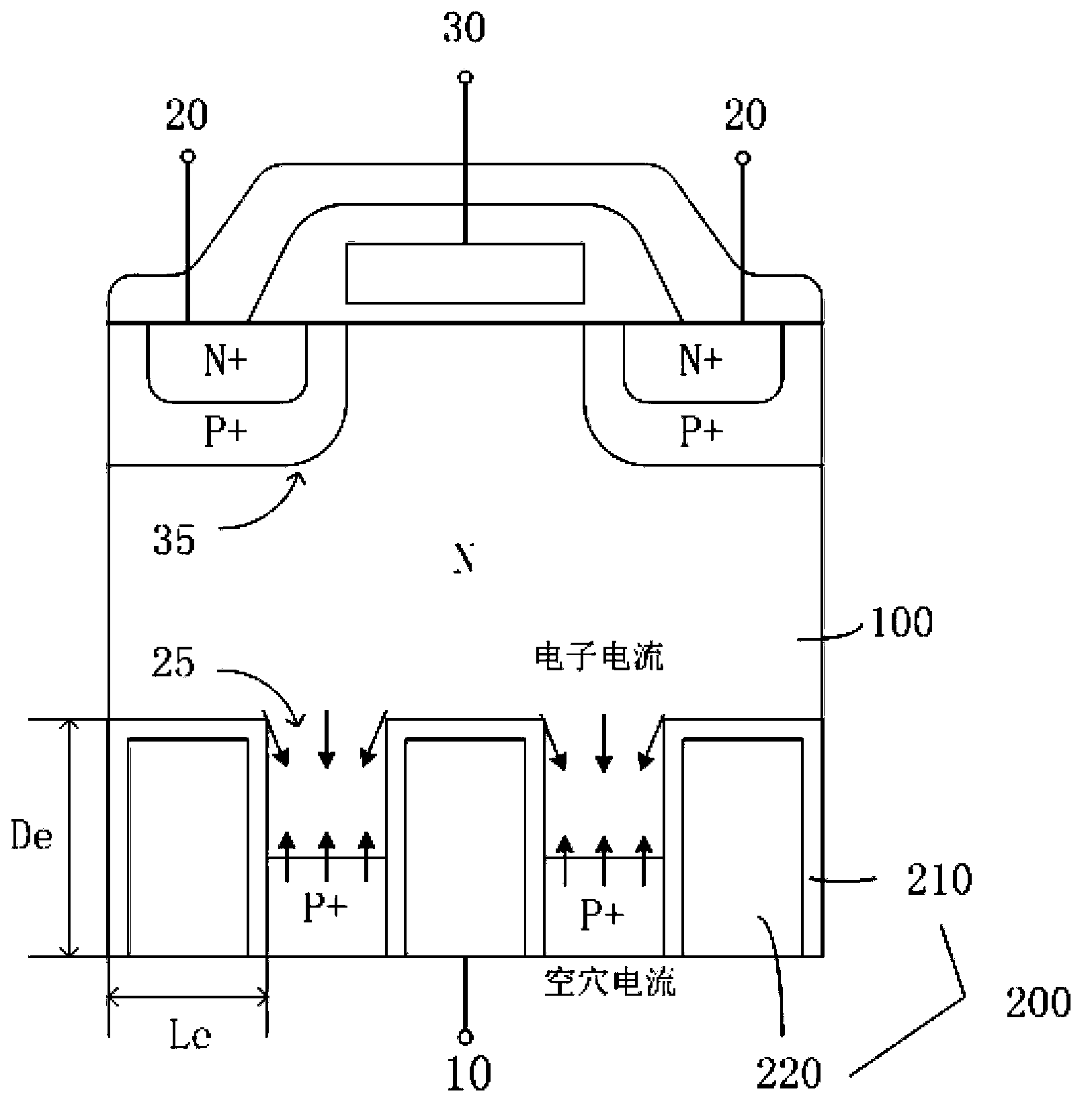
[0035] Such as figure 1 As shown, it is a schematic structural diagram of a general C-IGBT (Conventional-IGBT, traditional IGBT structure), such as figure 2 Shown is a schematic structural diagram of an insulated gate bipolar transistor (EEC-IGBT, Electronic Enhance Collector IGBT, electron-enhanced collector structure) provided in this embodiment. figure 1 As can be seen in the figure, a general C-IGBT structure is composed of a MOS structure 35 formed on the semiconductor substrate 100 and a PN junction 25 formed at the bottom of the semiconductor substrate 100 . The gate portion of the MOS transistor in the MOS structure 35 constitutes the gate 30 of the C-IGBT, the source and drain portions of the MOS transistor in the MOS structure 35...


PUM

PropertyMeasurementUnit
Widthaaaaaaaaaa
Depthaaaaaaaaaa

Abstract

Provided is an IGBT and a manufacture method thereof. The IGBT is formed on a semiconductor substrate, and comprises an MOS structure placed at the surface of the semiconductor substrate and a PN junction placed at the bottom of the semiconductor substrate. Multiple grooved structures are placed at the bottom of the semiconductor substrate, penetrate P and N zones of the PN junction, and divide the PN junction into multiple areas. Each grooved structure comprises a metal block at the bottom of the semiconductor substrate and an oxidation layer between the metal block and the semiconductor substrate, and the work function of metal of the metal block is lower than that of a material of the semiconductor substrate. The grooved structures enable that the direction and distribution of electronic current and hole current in the PN junction of the semiconductor substrate are changed, distribution of carriers in the semiconductor substrate can be adjusted by adjusting the grooved structures, and thus, the relation between the connecting voltage drop and turnoff time of the IGBT can be optimized.

Description

technical field [0001] The invention relates to the technical field of semiconductors, in particular to an insulated gate bipolar transistor and a manufacturing method thereof. Background technique [0002] IGBT (Insulated Gate Bipolar Transistor, insulated gate bipolar transistor) is composed of MOS (metal-oxide-semiconductor, insulated gate field effect transistor) and BJT (Bipolar Junction Transistor, bipolar transistor) located under the MOS channel Composite fully controlled voltage-driven power semiconductor device. It has the characteristics of high input impedance, small switching loss, fast speed, low voltage drive power, etc., and is widely used in high voltage, high current, high power and medium to high frequency occasions. [0003] However, due to the introduction of the PN junction hole injection mechanism of the IGBT substrate, the IGBT also has two problems: [0004] 1. There is a parasitic thyristor structure inside the device. Under certain conditions, th...

Claims


Application Information

Patent Timeline
IPC IPC(8): H01L29/739H01L29/06H01L21/331
CPCH01L29/7396H01L29/66325
Inventor 钟圣荣王根毅邓小社
Owner CSMC TECH FAB2 CO LTD
Why Eureka
Try Eureka