PN-structured gate demodulation pixel
A technology for demodulating pixels and gate layers, which is applied in the field of demodulating pixels with PN structure gates, and can solve the problems of being unable to be controlled, not causing perfect constant gradients, and being inflexible.
- Summary
- Abstract
- Description
- Claims
- Application Information
AI Technical Summary
Problems solved by technology
Method used
Image

Examples
Embodiment Construction
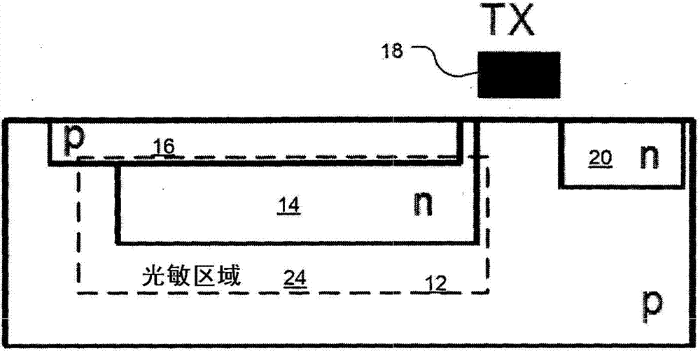
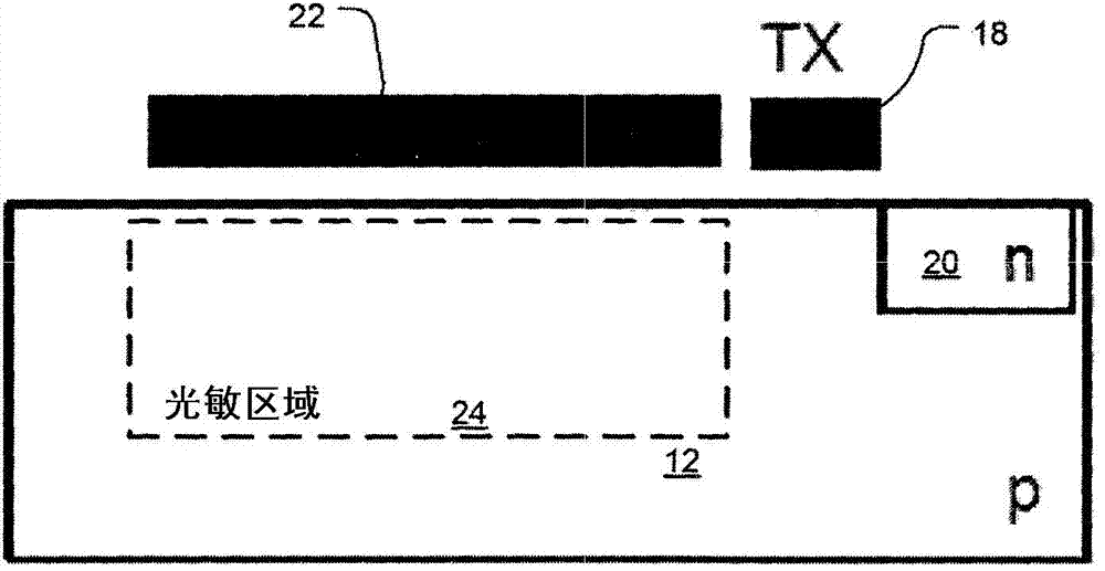
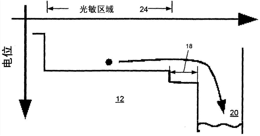
[0044] exist Figure 6 The basic idea of the invention in combination with an arbitrary arrangement according to an implementation of the invention is shown in . In the particular illustrated example, a P-type substrate 12 is used. However, in other examples, an N-type substrate is used. Gate 22 is deposited and subsequently formed on substrate 12 and is electrically isolated from the substrate by insulating layer 112 .
[0045] The single gate 12 is configured with N-type and P-type regions 110-1 to 110-n, wherein the distance between these regions may vary from zero to several millimeters. By applying appropriate voltages to the N-type and / or P-type gate regions 110 - 1 to 110 - n , CCD-like voltage distribution control can be obtained, which enables CCD-like charge transport in the semiconductor bulk material 12 . Every region or only a few regions between the N-type and P-type doped regions are in some examples low concentration N-type or P-type doped or intrinsic reg...
PUM
 Abstract
Description
Claims
Application Information
 - Generate Ideas
- Intellectual Property
- Life Sciences
- Materials
- Tech Scout
- Unparalleled Data Quality
- Higher Quality Content
- 60% Fewer Hallucinations
Browse by: Latest US Patents, China's latest patents, Technical Efficacy Thesaurus, Application Domain, Technology Topic, Popular Technical Reports.
© 2025 PatSnap. All rights reserved.Legal|Privacy policy|Modern Slavery Act Transparency Statement|Sitemap|About US| Contact US: help@patsnap.com