

Manufacture method of silicon epitaxial slice for fast recovery diode
A silicon epitaxial wafer, fast recovery technology, applied in semiconductor/solid-state device manufacturing, electrical components, circuits, etc., can solve the problems of difficult epitaxial layer process, difficulty in preparation of resistivity uniformity, etc., to promote device performance, crystal-free character defects, promote the effect of improvement
- Summary
- Abstract
- Description
- Claims
- Application Information
AI Technical Summary
Problems solved by technology
Method used
Image

Examples
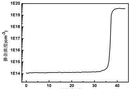
Embodiment 1
[0023] (1) First use HCl to etch the base of the epitaxial furnace at high temperature to remove the residual deposits on the base. The temperature is set at 1120°C, the flow rate of HCl gas is set at 3 L / min, and the etching time is set at It was set at 5 min, and then the base was re-wrapped with a layer of intrinsic polysilicon, the growth material was trichlorosilane gas, the flow rate was set at 35 g / min, and the time was set at 10 min.
[0024] (2) A silicon substrate is placed in the pit of the base of the epitaxial furnace. The conductivity type of the silicon wafer is N-type, the crystal orientation is , the resistivity is 0.002 Ω·cm, the thickness is 525 μm, and the diameter is 125 mm. The reaction chamber of the epitaxial furnace was purged with nitrogen and hydrogen in sequence for 10 minutes, and the gas flow rate was set at 100 L / min.
[0025] (3) Carry out vapor phase polishing on the surface of the silicon substrate, set the temperature at 1150 °C, use hydrogen...
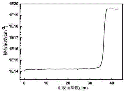
Embodiment 2
[0034] (1) First use HCl to etch the base of the epitaxial furnace at high temperature to remove the residual deposits on the base. The temperature is set at 1120°C, the flow rate of HCl gas is set at 2 L / min, and the etching time is set at It was set at 4 minutes, and then the base was re-coated with a layer of intrinsic polysilicon. The growth material was trichlorosilane gas, the flow rate was set at 35 g / min, and the time was set at 10 minutes.
[0035](2) A silicon substrate is placed in the pit of the base of the epitaxial furnace. The conductivity type of the silicon wafer is N-type, the crystal orientation is , the resistivity is 0.002 Ω·cm, the thickness is 525 μm, and the diameter is 125 mm. The reaction chamber of the epitaxial furnace was purged with nitrogen and hydrogen in sequence for 8 minutes, and the flow rate was set at 120 L / min.
[0036] (3) Perform vapor phase polishing on the surface of the silicon substrate, set the temperature at 1180 °C, use hydrogen ...
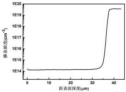
Embodiment 3
[0045] (1) First use HCl to etch the base of the epitaxial furnace at high temperature to remove the residual deposits on the base. The temperature is set at 1120°C, the flow rate of HCl gas is set at 3 L / min, and the etching time is set at It was set at 5 min, and then the base was re-wrapped with a layer of intrinsic polysilicon, the growth material was trichlorosilane gas, the flow rate was set at 35 g / min, and the time was set at 10 min.
[0046] (2) A silicon substrate is placed in the pit of the base of the epitaxial furnace. The conductivity type of the silicon wafer is N-type, the crystal orientation is , the resistivity is 0.002 Ω·cm, the thickness is 525 μm, and the diameter is 125 mm. The reaction chamber of the epitaxial furnace was purged with nitrogen and hydrogen in sequence for 8 minutes, the purity of nitrogen and hydrogen were both ≥99.999%, and the flow rate was set at 100 L / min.
[0047] (3) Perform vapor phase polishing on the surface of the silicon substr...
PUM
| Property | Measurement | Unit |
|---|---|---|
| Thickness | aaaaa | aaaaa |
| Diameter | aaaaa | aaaaa |
| Width | aaaaa | aaaaa |
Abstract
Description
Claims
Application Information