Preparation method of thin film transistor substrate, thin film transistor substrate and display device

A technology of thin-film transistors and substrates, which is applied in semiconductor/solid-state device manufacturing, electric solid-state devices, semiconductor devices, etc., can solve the problems of poor film-forming properties of source/drain material layers, lower device performance and yield, and uneven texture. To achieve the effect of ensuring the quality of the film layer, reducing lattice defects, and good film quality

Active Publication Date: 2021-08-27
SHENZHEN ROYOLE TECH CO LTD
View PDF3 Cites 0 Cited by
  • Summary
  • Abstract
  • Description
  • Claims
  • Application Information

AI Technical Summary

Problems solved by technology

[0003] In the prior art, the interlayer dielectric layer 150 is usually a single-layer silicon oxide layer, which is formed at one time by a CVD process. The disadvantage of the prior art is that the film-forming property of the silicon oxide layer at the corner of the step of the gate 140 is poor, specifically It is manifested as unevenness, uneven texture, and many lattice defects, which lead to poor film formation of the source / drain material layer deposited above it, and there are many lattice defects, so that when the source / drain material layer is etched The drain material (SD) layer is difficult to be etched when forming the source 161 and the drain 162, forming SD residues 200 protruding outward (see image 3 ),like figure 2 and image 3 As shown, SD residue 200 will seriously cause short circuit of the device, reducing device performance and yield

Method used


Image

  • Preparation method of thin film transistor substrate, thin film transistor substrate and display device
  • Preparation method of thin film transistor substrate, thin film transistor substrate and display device
  • Preparation method of thin film transistor substrate, thin film transistor substrate and display device

Examples


Embodiment Construction

[0033] The following will clearly and completely describe the technical solutions in the embodiments of the present invention with reference to the accompanying drawings in the embodiments of the present invention. Obviously, the described embodiments are only some, not all, embodiments of the present invention. Based on the embodiments of the present invention, all other embodiments obtained by persons of ordinary skill in the art without creative efforts fall within the protection scope of the present invention.

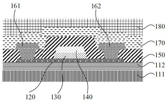
[0034] refer to Figure 4~Figure 11 , the invention discloses a method for preparing a thin film transistor substrate, comprising the following steps:

[0035] Step S1: Reference Figure 4 An active layer 20 is laminated on the substrate 10, the active layer 20 has a gate region, a source region and a drain region, and a gate insulating layer 30 and a gate layer 40 are sequentially laminated on the gate region of the active layer 20.

[0036] In a specific embodi...


PUM

PropertyMeasurementUnit
thicknessaaaaaaaaaa
thicknessaaaaaaaaaa
thicknessaaaaaaaaaa

Abstract

The invention discloses a preparation method of a thin film transistor substrate, the thin film transistor substrate and a display device. The preparation method of the thin film transistor substrate comprises the following steps that stacking an active layer, a gate insulating layer and a gate layer sequentially on a substrate; stacking a first interlayer dielectric layer, a second interlayer dielectric layer and a third interlayer dielectric layer sequentially, wherein the first interlayer dielectric layer and the second interlayer dielectric layer are both made of silicon oxide, and the content of oxygen in the material of the first interlayer dielectric layer is larger than that of oxygen in the material of the second interlayer dielectric layer, the third interlayer dielectric layer is made of silicon nitride or silicon oxynitride; forming a source contact hole and a drain contact hole; forming a source/drain material layer; forming a source electrode and a drain electrode; and removing the third interlayer dielectric layer to obtain the thin film transistor substrate. According to the invention, SD residue can be avoided.

Description

technical field [0001] The present invention relates to the technical field of thin film transistors (TFT), and more particularly, to a method for preparing a thin film transistor substrate, a thin film transistor substrate and a display device. Background technique [0002] refer to figure 1 , in the prior art, a thin film transistor (TFT) substrate includes a substrate 111, a buffer layer 112 formed above the substrate 111, an active layer 120, a gate insulating layer 130 and a gate layer 140 sequentially stacked above the buffer layer 112 , and the interlayer dielectric layer 150 . The interlayer dielectric layer 150 covers the entire surfaces of the gate layer 140, the gate insulating layer 130 and the active layer 120, and a source contact hole (corresponding to the source 161) and a drain contact hole (corresponding to the drain electrode 161) are respectively formed in the interlayer dielectric layer 150. electrode 162), exposing the active layer 120, depositing a s...

Claims


Application Information

Patent Timeline
Patent Type & Authority Applications(China)
IPC IPC(8): H01L21/77H01L27/12
CPCH01L27/1214H01L27/1248H01L27/1259
Inventor 彭蓉晏国文
Owner SHENZHEN ROYOLE TECH CO LTD
Why Eureka
Try Eureka