

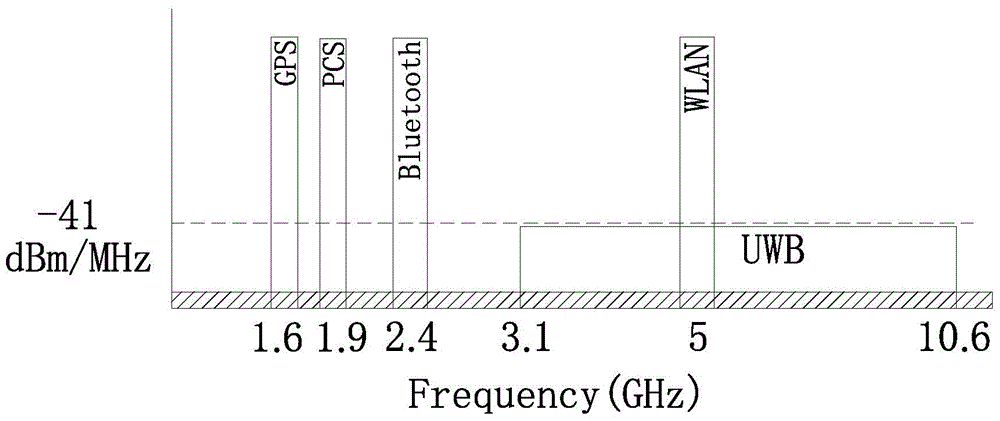
A substrate-integrated waveguide bandpass filter applied to wlan system
A substrate-integrated waveguide and band-pass filter technology, applied in the field of wireless communication, can solve problems such as difficult design and processing, complex structure, etc., and achieve the effect of overcoming large loss, high selectivity, and high cost
- Summary
- Abstract
- Description
- Claims
- Application Information
AI Technical Summary
Problems solved by technology
Method used
Image

Examples
Embodiment 1
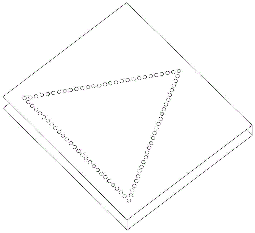
[0048] This embodiment designs a basic substrate integrated waveguide bandpass filter, such as Figure 6 As shown, the filter includes a substrate-integrated waveguide (SIW), and the substrate-integrated waveguide includes a dielectric substrate 1 and two layers of metal patches arranged on the front and back of the dielectric substrate 1 (the metal patches on the front are marked with numbers 2. The metal patch on the reverse side is not shown in the figure, and the embodiment 2 and 3 are the same) and several metal through holes 3, and the several metal through holes 3 pass through the metal patch 2 on the front side of the dielectric substrate 1, the dielectric The metal patch on the back side of the substrate 1 and the dielectric substrate 1, the metal through holes 3 surround the metal patch 2 on the front side of the dielectric substrate 1 to form two rectangular cavities (upper and lower rectangular cavities) of the same size. body marked number 4, lower rectangular cav...
Embodiment 2
[0053] This embodiment also designs a basic substrate integrated waveguide bandpass filter, such as Figure 11 As shown, the difference between the structure of this filter and Embodiment 1 is that: the left side of the upper rectangular cavity 4 is provided with a first feeder 6, and the left side of the lower rectangular cavity 5 is provided with a second feeder 7, also That is to say, the first feeder 6 and the second feeder 7 are located on the same side.
[0054] Such as Figure 12 As shown, the S parameters of the above structure (S 11 parameter refers to the return loss of the input port, S 21 The parameter refers to the forward transmission coefficient from the input port to the output port) In the response, it can also be seen that the passband center frequency of the filter is 4.3GHz, and the passband is formed by using the TE of the substrate integrated waveguide 101 mode, but compared with the simulation curve of the structure of embodiment 1, a pair of transmis...
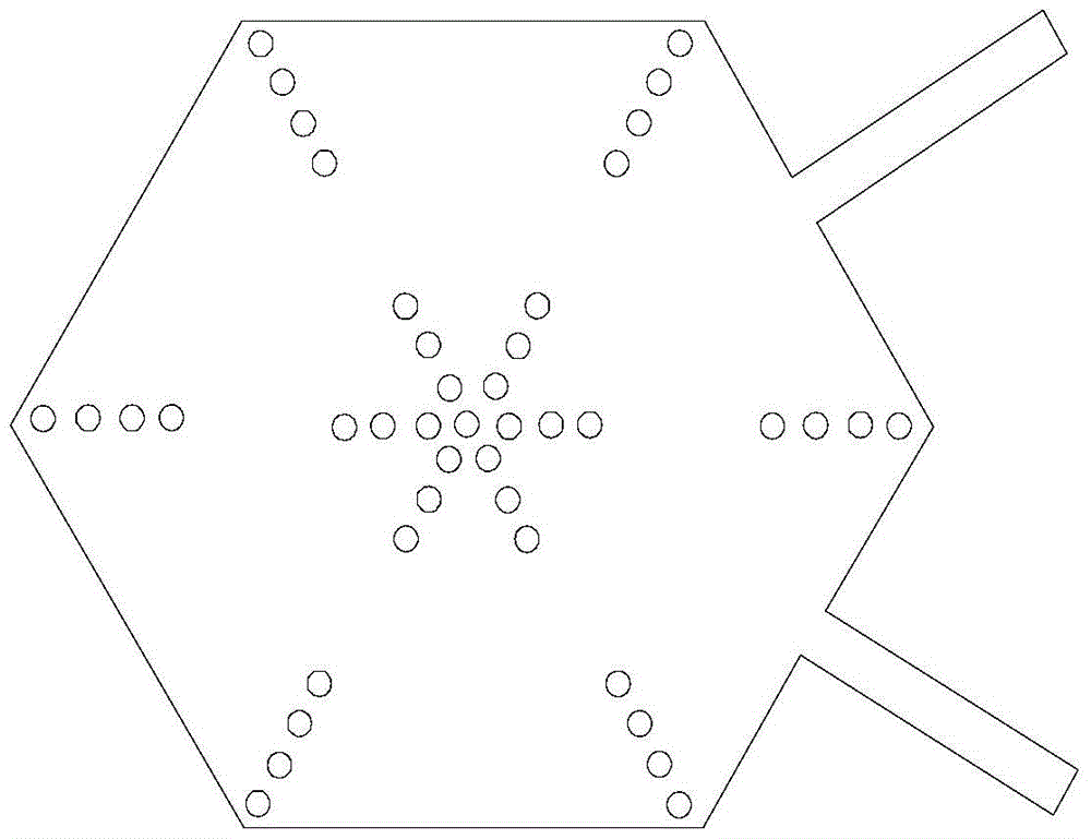
Embodiment 3
[0057] In Example 2 of Figure 13 On the basis of the structure, make improvements to the feeder part, such as Figure 15 As shown, the first branch 10 is loaded on the first feeder 6, the second branch 11 is loaded on the second feeder 7, the first branch 10 extends downward, the second branch 11 extends upward, and the first branch 11 The node 10 and the second branch 11 do not overlap with each other, and the source-load coupling is used to increase the transmission zero point and improve the selectivity of the filter, which from Figure 16 (The dotted line represents the simulation result of unloaded branches, and the solid line represents the simulation results of loaded branches). It can be seen that after loading branches, S 21 The parameter adds a pair of transmission zeros near 5.3GHz, which reduces the out-of-band attenuation from about 20dB to below 35dB, improving the filter squareness, that is, improving the selectivity of the filter.
[0058] To verify the abov...
PUM
 Abstract
Description
Claims
Application Information