Image sensor and formation method thereof

A technology of image sensor and pixel unit, which is applied in the semiconductor field to achieve the effect of reducing pixel area, improving performance, and increasing fill factor

Active Publication Date: 2015-02-04
GALAXYCORE SHANGHAI
View PDF7 Cites 4 Cited by
  • Summary
  • Abstract
  • Description
  • Claims
  • Application Information

AI Technical Summary

Problems solved by technology

[0004] The performance of existing image sensors still needs to be further improved

Method used


Image

  • Image sensor and formation method thereof
  • Image sensor and formation method thereof
  • Image sensor and formation method thereof

Examples


Embodiment Construction

[0052] As described in the background art, the performance of the existing image sensor needs to be further improved.

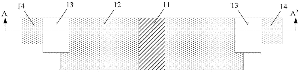
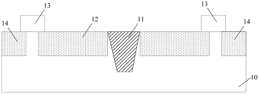
[0053] Please refer to figure 2 with image 3 , Are respectively a top view and a cross-sectional view of the photodiodes and transfer transistors of adjacent pixels located in the same row in the pixel array in the prior art, image 3 For the edge figure 2 A schematic cross-sectional view of the secant line AA'.

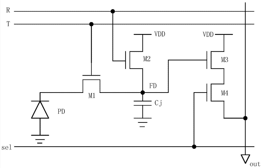
[0054] The image sensor unit includes a photodiode 12 in a semiconductor substrate 10, a gate structure 13 of a transfer transistor on the semiconductor substrate 10 on one side of the photodiode 12, and a semiconductor on the other side of the gate structure 13 The floating diffusion region 14 in the substrate 10. The pixel unit of the image sensor also includes other parts, such as: reset transistor, source follower transistor, row gate transistor, etc. figure 2 Part not shown in.

[0055] A shallow trench isolation structure 11 is formed in the sem...


PUM


Abstract

The invention discloses an image sensor and a formation method thereof. The image sensor comprises a semiconductor substrate; a shallow trench isolation structure disposed in the semiconductor substrate; photodiodes disposed in the semiconductor substrate at the two sides of the shallow trench isolation structure; a groove disposed in the shallow trench isolation structure, the side wall of the groove exposing a part of the semiconductor substrate; and a grid structure disposed in the groove, the side wall of the grid structure being disposed on the surface of the side wall of the groove. The fill factor of the image sensor is improved.

Description

Technical field [0001] The present invention relates to the field of semiconductor technology, in particular to an image sensor and a forming method thereof. Background technique [0002] Image sensors are semiconductor devices that convert optical image signals into electrical signals. Products with image sensors as key components have become the current and future industry's attention, attracting investment from many manufacturers. In terms of product categories, image sensor products are mainly divided into charge-coupled device image sensor (CCD image sensor) and complementary metal oxide image sensor (CMOS sensor). CMOS image sensor is a fast-developing solid-state image sensor. Because the image sensor part and the control circuit part of the CMOS image sensor are integrated in the same chip, the CMOS image sensor is small in size, low in power consumption, and low in price. The traditional CCD (charge coupled) image sensor has more advantages and is easier to popularize....

Claims


Application Information

Patent Timeline
Patent Type & Authority Applications(China)
IPC IPC(8): H01L27/146
Inventor 李杰李文强
Owner GALAXYCORE SHANGHAI
Why Eureka
Try Eureka