
Optical device wafer processing method

一种加工方法、光器件的技术,应用在半导体器件、金属加工设备、半导体/固态器件制造等方向,能够解决降低光器件品质、碎屑飞散、生产效率差等问题,达到生产效率良好的效果

Active Publication Date: 2015-02-11
DISCO CORP
View PDF10 Cites 15 Cited by
  • Summary
  • Abstract
  • Description
  • Claims
  • Application Information

AI Technical Summary

Problems solved by technology

[0007] However, in order to position the condensing point of the laser light inside the wafer to form the modified layer, it is necessary to use a condensing lens with a numerical aperture (NA) of about 0.8. For example, to divide a 300 μm thick wafer into individual devices, It must be formed as overlapping multi-layer modified layers, and there is a problem of poor production efficiency
[0008] In addition, if the wafer is irradiated with pulsed laser light having an absorbing wavelength, the ablation process will be performed near the irradiated surface of the wafer, and the energy will not penetrate into the inside of the wafer. Therefore, it is necessary to irradiate the pulsed laser light multiple times along the planned dividing line. Light, poor production efficiency, and there is a problem of flying debris and reducing the quality of optical devices

Method used


Image

  • Optical device wafer processing method
  • Optical device wafer processing method
  • Optical device wafer processing method

Examples


Embodiment Construction

[0036] Hereinafter, the wafer processing method of the present invention will be described in more detail with reference to the drawings.

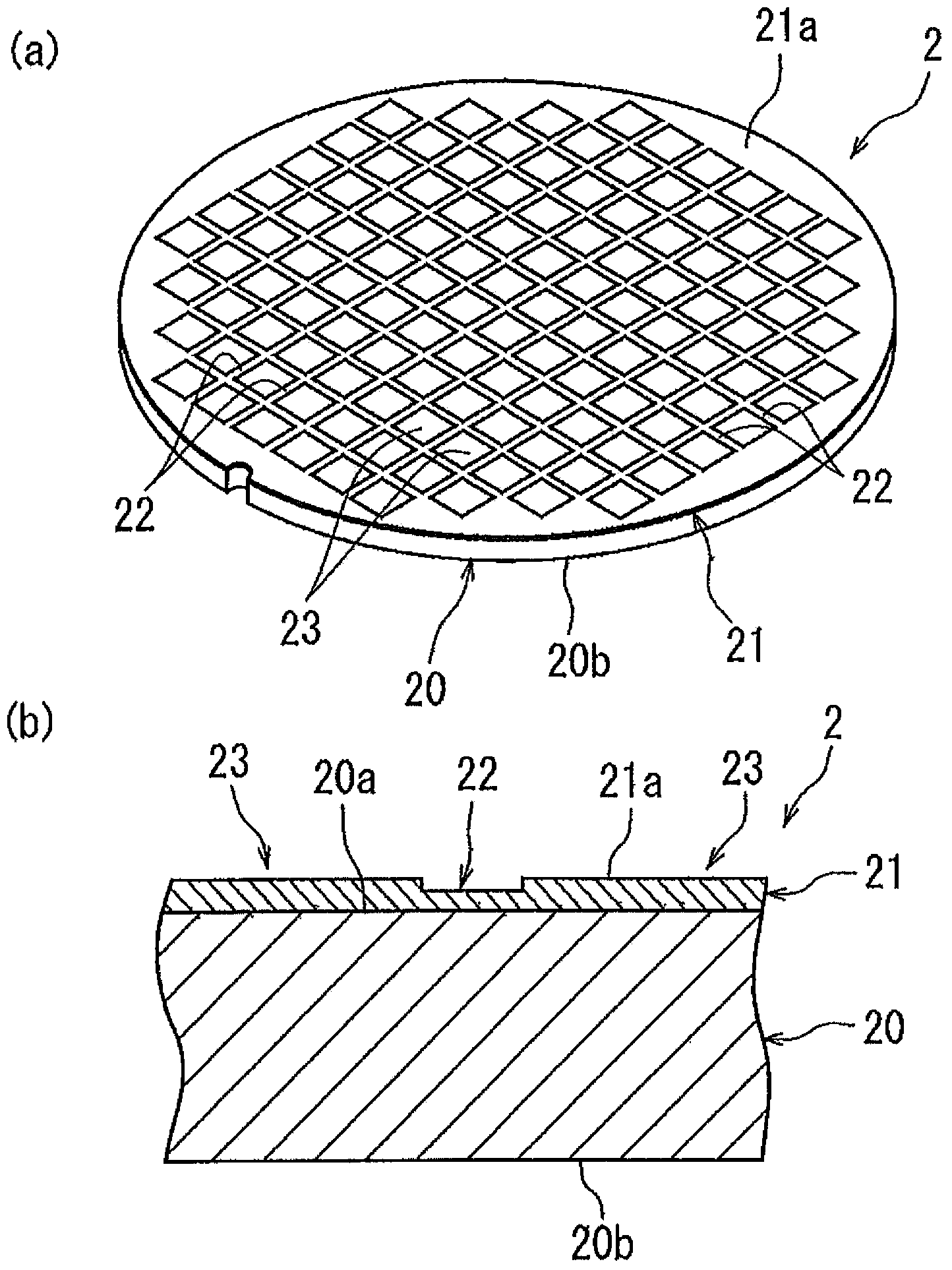
[0037] figure 1 (a) and (b) show enlarged perspective views and cross-sectional views of main parts of an optical device wafer divided into individual optical devices by the wafer processing method of the present invention. figure 1 In the optical device wafer 2 shown in (a) and (b), a light emitting layer (epitaxial layer) 21 made of a nitride semiconductor is laminated on the front surface 20a of a sapphire substrate 20 which is a single crystal substrate with a thickness of 300 μm. Further, the light emitting layer (epitaxial layer) 21 is divided by a plurality of dividing lines 22 formed in a grid pattern, and optical devices 23 such as light emitting diodes and laser diodes are formed in the divided regions.

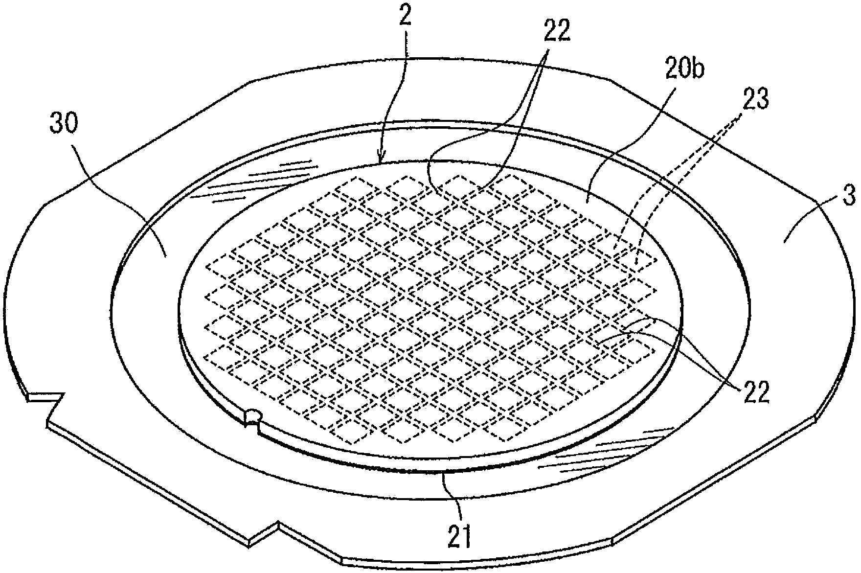
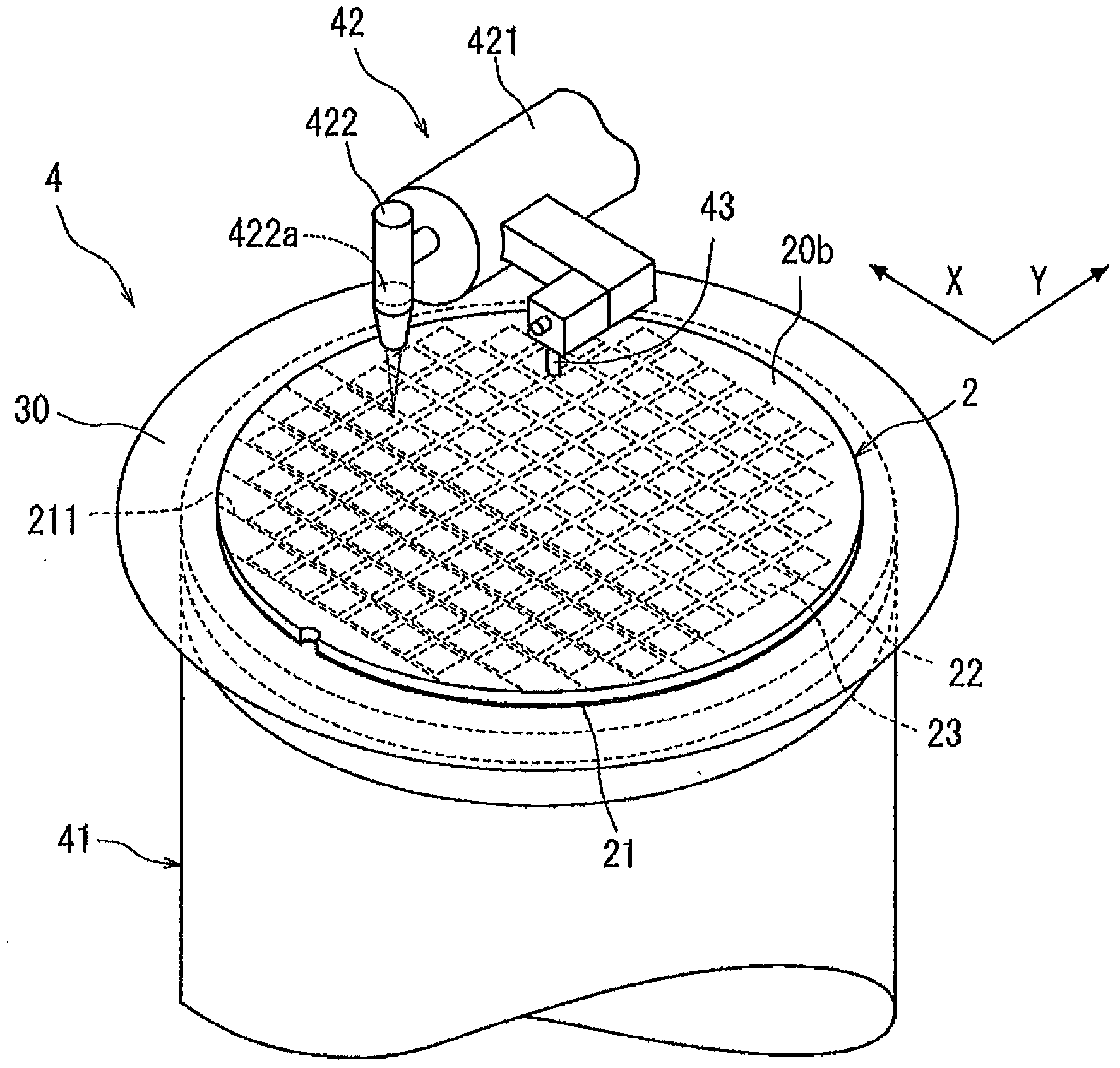
[0038] In order to divide the above-mentioned optical device wafer 2 along the planned dividing line 22, first, a wafer suppo...


PUM


Abstract

In an optical device wafer processing method, a light emitting layer on the front side of a wafer is removed by applying a pulsed laser beam to the wafer along division lines from the back side of a substrate with the focal point of the beam set near the light emitting layer, thereby partially removing the light emitting layer along the division lines. A shield tunnel is formed by applying the beam to the wafer along the division lines from the back of the substrate with the focal point of the beam set near the front of the substrate. This forms a plurality of shield tunnels arranged along each division line, each shield tunnel extending from the front side of the substrate to the back side thereof. Each shield tunnel has a fine hole and an amorphous region formed around the fine hole for shielding the fine hole.

Description

technical field [0001] The present invention relates to a processing method for an optical device wafer as follows: the optical device wafer is divided into individual optical devices along a predetermined dividing line, wherein the optical device wafer is as follows: sapphire (Al 2 o 3 ) substrates, silicon carbide (SiC) substrates, and other single-crystal substrates on which light-emitting layers are stacked, and optical devices such as light-emitting diodes and laser diodes are formed in multiple regions divided by a plurality of planned division lines formed in a grid pattern. . Background technique [0002] In the manufacturing process of optical devices, in sapphire (Al 2 o 3 ) substrates, silicon carbide (SiC) substrates, and other single-crystal substrates, where a light emitting layer composed of an n-type nitride semiconductor layer and a p-type nitride semiconductor layer is laminated, and is divided by a plurality of dividing lines formed in a grid pattern. ...

Claims


Application Information

Patent Timeline
Patent Type & Authority Applications(China)
IPC IPC(8): B23K26/38B23K26/402B23K26/064H01L33/00H01L21/78
CPCH01L21/2686H01L33/0095H01L21/78
Inventor 武田昇森数洋司
Owner DISCO CORP
Learn More