Radio frequency LDMOS device and manufacture method
A device and radio frequency technology, which is applied in semiconductor/solid-state device manufacturing, semiconductor devices, electrical components, etc., can solve the problems of large on-resistance, low concentration of drift area, etc., achieve low on-resistance, uniform drift area, and reduce leakage The effect of current
- Summary
- Abstract
- Description
- Claims
- Application Information
AI Technical Summary
Problems solved by technology
Method used
Image
Examples
Embodiment Construction
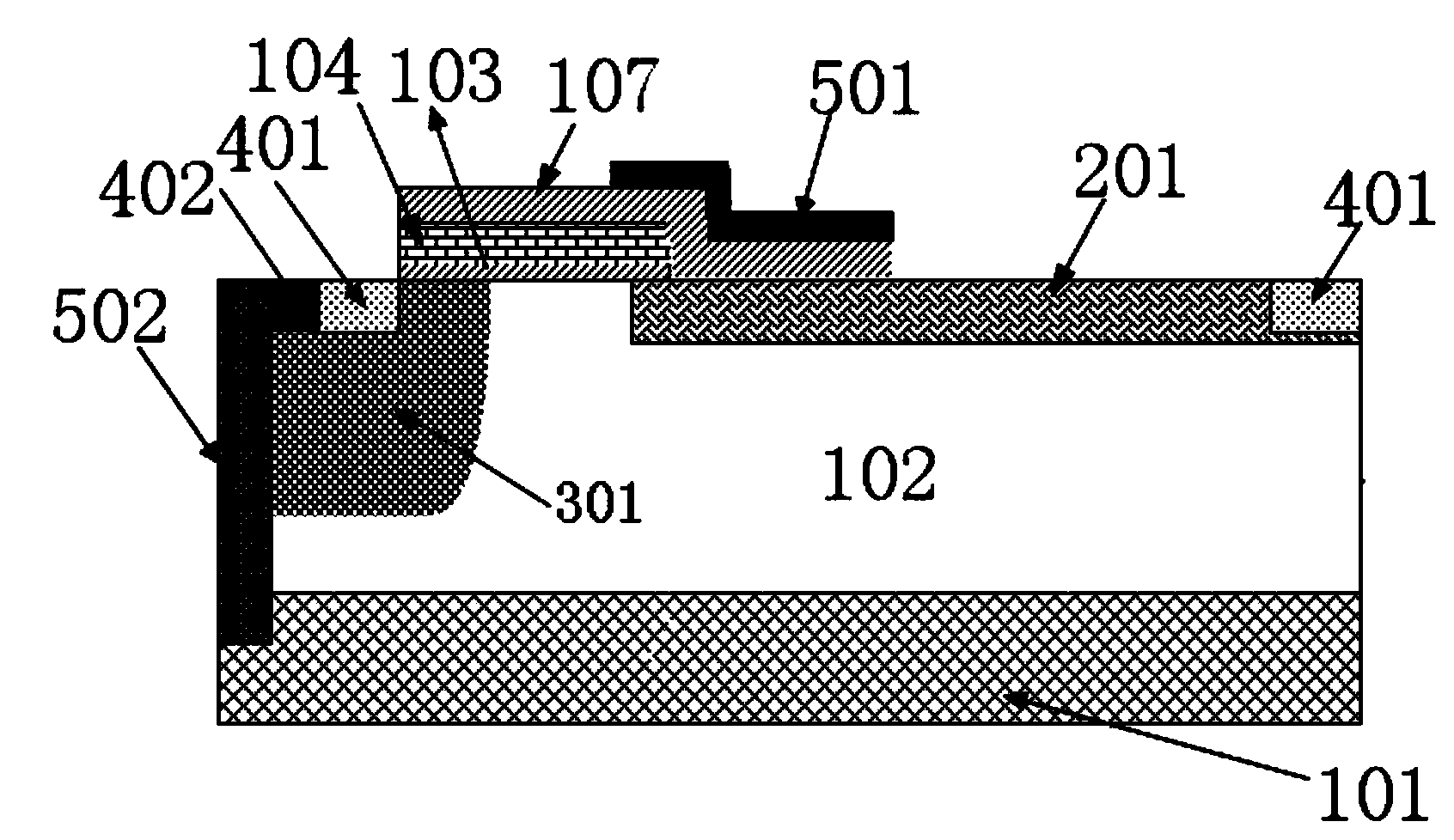
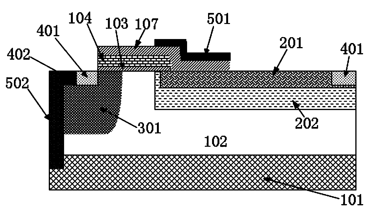
[0027] The radio frequency LDMOS device described in the present invention, such as figure 2 As shown, on the P-type substrate 101 is a P-type epitaxy 102, the P-type epitaxy 102 has a P-type body region 301, and the P-type body region 301 has the source region of the LDMOS device and is in contact with the source region heavily doped P-type region 402 .
[0028] The RF P-type epitaxy 102 also has lightly doped drift regions 201 and 202, which are formed by two implants. The first ion implantation forms the lightly doped drift region 201, and the second ion implantation forms the lightly doped drift region 201. impurity drift region 202 . The lightly doped drift region 202 also has a drain 401 of the LDMOS device.
[0029] The silicon surface between the P-type body region 301 and the lightly doped drift region 202 has a gate oxide 103 and a polysilicon gate 104; the silicon surface of the polysilicon gate 104 and the lightly doped drift region 202 close to the polysilicon ...
PUM
 Abstract
Description
Claims
Application Information


