Manufacturing method of tunneling field effect transistor

A technology of tunneling field effect and manufacturing method, which is applied in transistors, semiconductor/solid-state device manufacturing, diodes, etc., can solve problems such as difficult to realize narrow tunneling junctions, destroy sub-threshold swings, and difficult to turn off devices, and achieve Improve subthreshold characteristics, reduce leakage current, and increase the effect of on-current

Active Publication Date: 2017-01-04
INST OF MICROELECTRONICS CHINESE ACAD OF SCI
View PDF5 Cites 0 Cited by
  • Summary
  • Abstract
  • Description
  • Claims
  • Application Information

AI Technical Summary

Problems solved by technology

However, in order to reduce the sub-threshold swing and increase the conduction current, the tunneling junction needs to be as narrow as possible. However, the tunneling field effect transistor with the existing structure will always cause the diffusion distribution of impurities during the injection and heat treatment process, and it is difficult to achieve a narrow tunneling junction. tunneling junction
[0005] In addition, in conventional tunneling field effect transistors, the source and drain regions are highly doped, and doping will inevitably introduce defects, and the leakage current associated with defects will destroy the reduction of subthreshold swing.
Moreover, conventional tunneling field effect transistors have bipolar characteristics that can be turned on at both positive and negative gate voltages, making it difficult to completely turn off the device

Method used


Image

  • Manufacturing method of tunneling field effect transistor
  • Manufacturing method of tunneling field effect transistor
  • Manufacturing method of tunneling field effect transistor

Examples


Embodiment Construction

[0040] Embodiments of the present invention are described in detail below, examples of which are shown in the drawings, wherein the same or similar reference numerals designate the same or similar elements or elements having the same or similar functions throughout. The embodiments described below by referring to the figures are exemplary only for explaining the present invention and should not be construed as limiting the present invention.

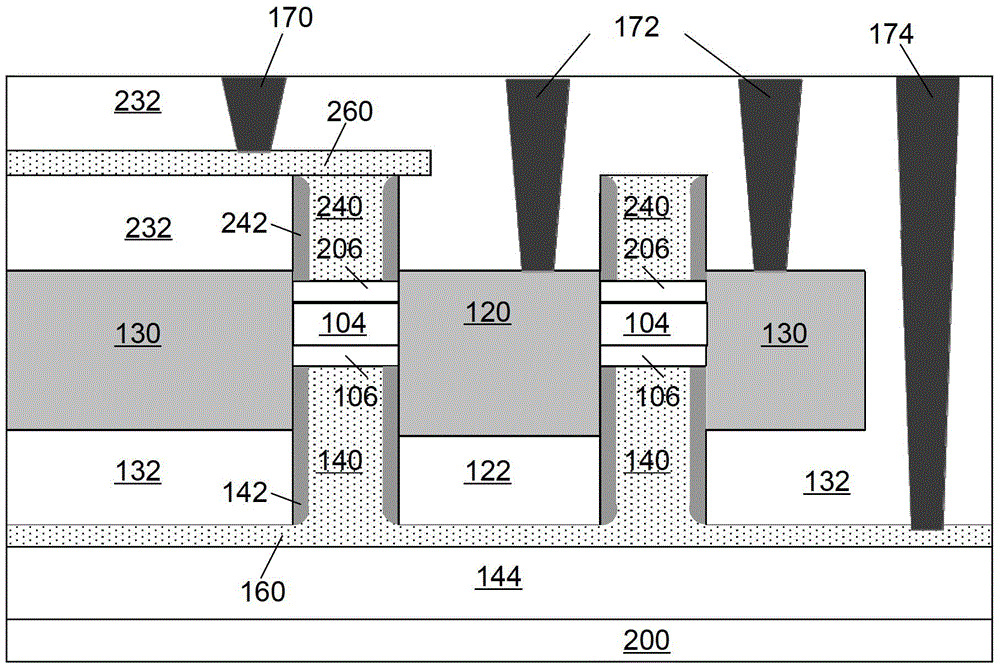
[0041] The present invention aims to propose a new tunneling field effect transistor structure to overcome the difficulty in realizing narrow tunneling junctions in existing tunneling field effect transistor structures. Refer to figure 1 As shown, the tunneling field effect transistor includes:

[0042] semiconductor layer 104;

[0043] The first gate dielectric layer 106 and the second gate dielectric layer 206 are respectively located on two opposite surfaces of the semiconductor layer 104;

[0044] The source region 120 and the drai...


PUM


Abstract

The invention provides a tunneling field effect transistor. The tunneling field effect transistor comprises a semiconductor layer, a first gate medium layer and a second gate medium layer which are respectively arranged two opposite surfaces of the semiconductor layer, a source electrode region and a drain electrode region which have different doping types, are respectively arranged at two sides of the semiconductor layer and contact with the semiconductor layer, and a first grid electrode and a second grid electrode which are respectively arranged on the first gate medium layer and the second gate medium layer. According to the tunneling field effect transistor, tunneling junctions are controlled through thickness of a channel region, a larger effective tunneling area is realized, the conduction current is further enhanced, moreover, tunneling is generated in the semiconductor layer, namely, the channel; tunneling layers are non-doped or low-doped tunneling layers, so a leakage current caused by defects can be reduced, and thereby sub-threshold characteristics of devices can be improved; dual-gate control is employed, so bipolar conduction characteristics can be better controlled, and on and off control on the devices can be realized.

Description

technical field [0001] The invention relates to the field of semiconductor devices, in particular to a manufacturing method of a tunneling field effect transistor. Background technique [0002] With the continuous shrinking of the device size, the number of devices per unit area of ​​the chip is increasing, and how to reduce power consumption has become an increasingly prominent problem. [0003] The structure of a conventional tunneling field-effect transistor (Normal-TFET) mainly includes a substrate (channel), a gate dielectric layer, a gate, and source / drain regions on both sides of the gate, mainly based on the quantum tunneling effect. P-type tunneling field effect transistor is taken as an example. When a negative voltage is applied to the gate, the potential of the channel region increases, and quantum tunneling occurs from the source region to the channel region. The electrons and holes generated by the tunneling pass from the source region to the drain region area...

Claims


Application Information

Patent Timeline
Patent Type & Authority Patents(China)
IPC IPC(8): H01L29/786H01L29/08H01L29/423H01L21/336
CPCH01L29/0895H01L29/66356H01L29/7391
Inventor 朱正勇朱慧珑许淼
Owner INST OF MICROELECTRONICS CHINESE ACAD OF SCI
Why Eureka
Try Eureka