Junctionless Folded I-Gate Field Effect Transistor with Low Leakage Current

A field-effect transistor and low-leakage technology, applied in circuits, electrical components, semiconductor devices, etc., can solve the problems of increased static power consumption of devices, reduce static power consumption, increase effective channel length, and reduce manufacturing costs Effect

Active Publication Date: 2019-08-02
宿松新驱光电科技有限公司
View PDF3 Cites 0 Cited by
  • Summary
  • Abstract
  • Description
  • Claims
  • Application Information

AI Technical Summary

Problems solved by technology

Therefore, devices based on FinFETs structure will continue to increase the static power consumption of the device as the size is further reduced.

Method used


Image

  • Junctionless Folded I-Gate Field Effect Transistor with Low Leakage Current
  • Junctionless Folded I-Gate Field Effect Transistor with Low Leakage Current
  • Junctionless Folded I-Gate Field Effect Transistor with Low Leakage Current

Examples


Embodiment Construction

[0044] Below in conjunction with accompanying drawing, the present invention will be further described:

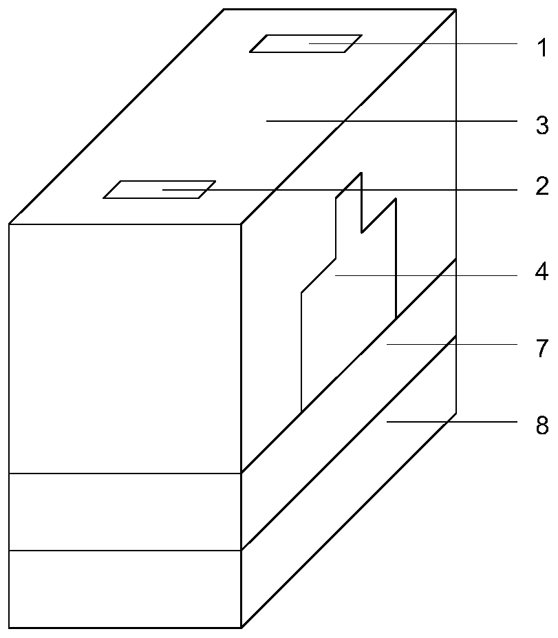
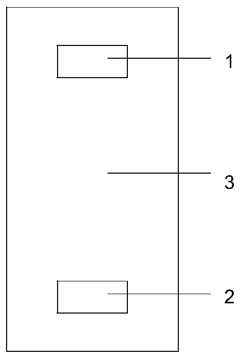
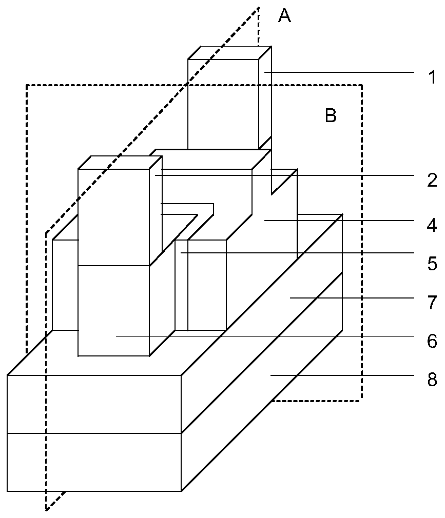
[0045]The present invention provides a junctionless folded I-shaped gate field effect transistor with low leakage current. The low leakage current property is realized through the control of carrier distribution in single crystal silicon by the I-shaped gate electrode 4 . Applying a positive voltage to the gate electrode 4 places the device in a conducting state. The folded I-shaped gate electrode 4 located on both sides of the single crystal silicon 6 respectively constitutes the upper and lower "horizontal" parts of the letter "I", and its length is longer, which mainly controls the carrier distribution in the single crystal silicon Function; while the folded I-shaped gate electrode 4 is located above the monocrystalline silicon 6 to form the middle "vertical" part of the letter "I", its length is relatively short, and it is located in the center of the monocrystalline s...


PUM


Abstract

The invention relates to a non-junction folded I-shaped gate field effect transistor with low leakage current, which comprises a silicon substrate of an SOI wafer. An insulation layer of the SOI wafer is arranged above the silicon substrate of the SOI wafer; monocrystalline silicon is arranged above the insulation layer of the SOI wafer; a gate dielectric insulation layer is attached to the surface of the monocrystalline silicon; a folded I-shaped gate electrode is attached to the surface of the gate dielectric insulation layer; the gate electrode is closely attached to the gate dielectric insulation layer; two ends of the upper surface of the monocrystalline silicon are respectively a source electrode and a drain electrode; adjacent monocrystalline silicon and the source electrode and the drain electrode are separated by insulation dielectric layers; and metal is injected to through holes formed after the insulation dielectric layers attached to the upper surface of the monocrystalline silicon and close to the two ends are etched to generate the source electrode and the drain electrode respectively. A low reverse leakage current characteristic can be provided in a condition of ensuring the positive characteristic not to be influenced almost, the power consumption of the device is reduced, and promotion and applications are facilitated.

Description

technical field [0001] The invention belongs to the field of ultra-large-scale integrated circuit manufacturing, in particular to a junction-free folded I-shaped gate field-effect transistor structure with low leakage current suitable for low-power integrated circuit manufacturing. Background technique [0002] According to the requirements of Moore's law, the basic unit MOSFET of integrated circuits will become smaller and smaller in size, which will not only make the manufacturing process more difficult, but also cause various adverse effects to become more prominent. On the one hand, the size is proportionally reduced, the channel is getting shorter and shorter, and the gate control ability is weakened, making it difficult for the device to work normally and turn off. On the other hand, the formation of steep PN junctions at the nanoscale requires extremely high heat treatment processes. The FinFETs structure based on multi-gate technology and junctionless field effect t...

Claims


Application Information

Patent Timeline
Patent Type & Authority Patents(China)
IPC IPC(8): H01L29/78H01L29/10H01L29/423H01L21/336
CPCH01L29/1033H01L29/42376H01L29/66666H01L29/7828H01L2029/7857
Inventor 刘溪杨光锐靳晓诗
Owner 宿松新驱光电科技有限公司
Why Eureka
Try Eureka