Tunneling Field Effect Transistor and Method of Forming the Same
A tunneling field effect, transistor technology, applied in semiconductor devices, semiconductor/solid-state device manufacturing, electrical components, etc., can solve the problem of leakage current destroying sub-threshold swing, difficult to achieve narrow tunneling junction, difficult to turn off devices, etc. problem, to achieve the effect of improving sub-threshold characteristics, reducing leakage current, and increasing on-current
- Summary
- Abstract
- Description
- Claims
- Application Information
AI Technical Summary
Problems solved by technology
Method used
Image
Examples
Embodiment 1
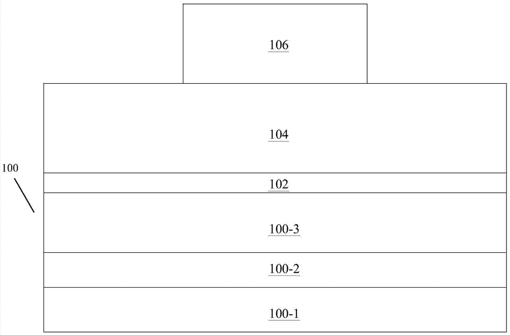
[0060] First, in step S101, an SOI substrate 100 is provided, referring to figure 1 shown.
[0061] The SOI substrate 100 is composed of the bottom silicon 100-1, the buried oxide layer 100-2 and the top silicon 100-3, and the fins are formed by the top silicon 100-3.
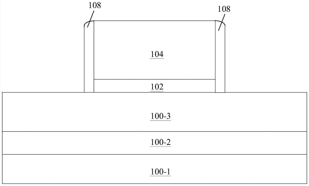
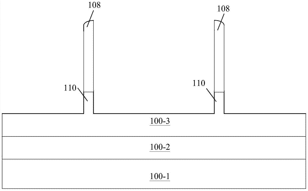
[0062] Next, in step S102 , the fins 110 are formed.
[0063] In the present invention, the width of the tunnel junction is controlled by the width of the fin. Of course, the narrower the tunnel junction, the better. The method proposed in this embodiment is especially suitable for the formation of narrow fins, for example, the width is about 10nm or narrower. the fins.
[0064] In this embodiment, the following steps are specifically included:
[0065] First, a silicon oxide layer 102 and a polysilicon layer 104 are sequentially deposited on a semiconductor substrate, and a photosensitive etchant 106 is formed on the polysilicon layer 104, such as figure 1 shown.
[0066] Next, etching is performed usin...
Embodiment 2
[0085] First, in step S201, an SOI substrate 200 is provided, referring to Figure 15 shown.
[0086] The SOI substrate 200 is composed of bottom silicon 200-1, buried oxide layer 200-2 and top silicon 200-3, and the fins are formed by top silicon 200-3.
[0087] Then, in step S202, a silicon oxide layer 202 and a polysilicon layer 204 are sequentially deposited on the semiconductor substrate, and a photosensitive etchant 206 is formed on the polysilicon layer 204, such as Figure 15 shown.
[0088] Next, in step S203, the polysilicon layer 204 is etched to form a patterned polysilicon layer 204, and a fin capping layer 214 is formed on the sidewall of the polysilicon layer 204, and a first gate capping layer is formed on the sidewall of the fin capping layer 214 212, such as Figure 16 shown.
[0089] In this embodiment, the fin capping layer 214 is silicon nitride with a width of less than 10 nm, the first gate capping layer 212 is SiGe, and the polysilicon layer 204 is ...
PUM
 Abstract
Description
Claims
Application Information


