Adulation method for MOS transistor body area

A MOS transistor and body region technology, which is applied in semiconductor/solid-state device manufacturing, electrical components, circuits, etc., can solve the problems of reduced carrier mobility, increased parasitic capacitance and leakage current, and poor subthreshold characteristics

Inactive Publication Date: 2009-11-18
SEMICON MFG INT (SHANGHAI) CORP +1
View PDF2 Cites 0 Cited by
  • Summary
  • Abstract
  • Description
  • Claims
  • Application Information

AI Technical Summary

Problems solved by technology

However, the continuous increase of doping concentration will lead to problems such as the decrease of carrier mobility, the deterioration of subthreshold characteristics, and the difficulty in reducing the threshold voltage.
The Halo (pocket) doping method alleviates the above problems to a certain extent, but there are still problems such as source-drain parasitic resistance, parasitic capacitance and leakage current increase.

Method used


Image

  • Adulation method for MOS transistor body area
  • Adulation method for MOS transistor body area
  • Adulation method for MOS transistor body area

Examples


Embodiment Construction

[0038] The preferred embodiment of the present invention is described in more detail below with reference to the accompanying drawings of the present invention.

[0039] (1) The substrate is a bulk silicon wafer

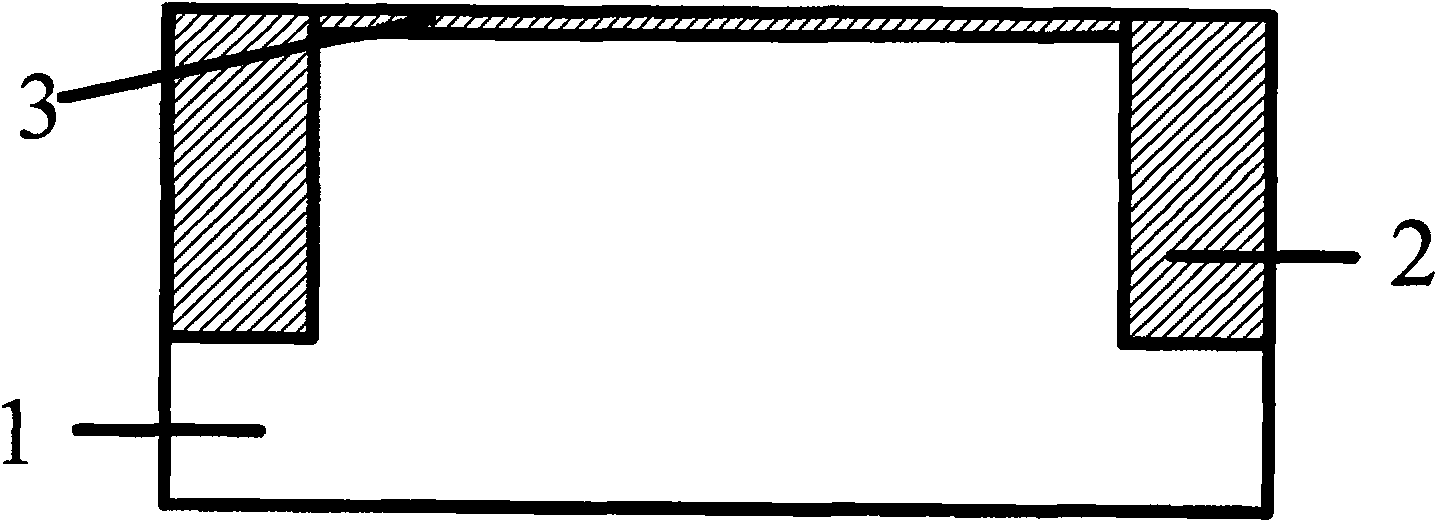
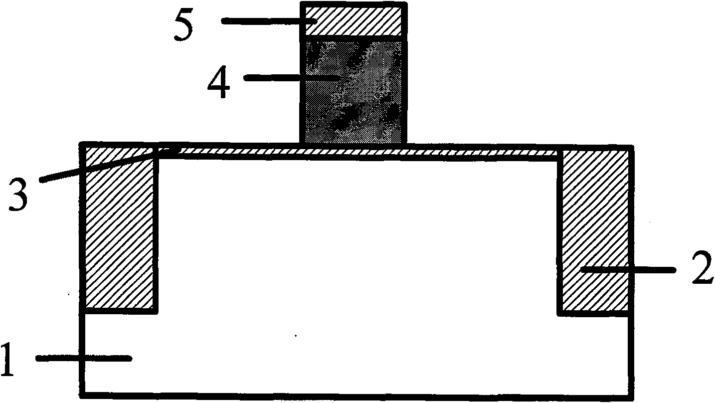
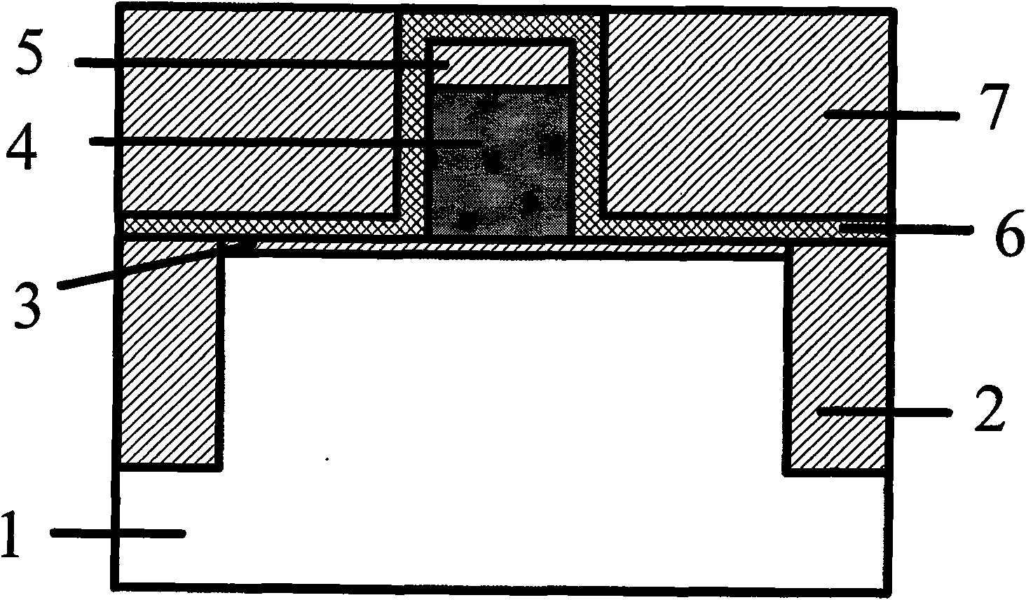
[0040] A specific example of the integrated silicon MOS transistor prepared by the manufacturing method is as follows: Figure 1 to Figure 6 shown, including the following steps:

[0041] 1) if figure 1 As shown, the crystal orientation of the single crystal silicon substrate used is (100), and for n-type MOS transistors, the body region 1 is initially lightly doped with p-type. For p-type MOS transistors, body region 1 is initially lightly doped with n-type. The active region isolation layer 2 is fabricated by using conventional CMOS shallow trench isolation technology. Next, a gate dielectric layer 3 is grown. The gate dielectric layer 3 is silicon dioxide with a thickness of 0.5-3 nm. The gate dielectric can also be formed by one of the following methods: c...


PUM


Abstract

The invention provides a method for doping a body region of a MOS transistor, belonging to the technical field of semiconductor integrated circuits and its manufacture. In the method, slits are formed on both sides of the gate electrode, and the ion implantation doping of the body region is performed through the slits. In the present invention, since the heavy doping of the body region is carried out through the slits on both sides of the gate electrode, the heavily doped region is strip-shaped on both sides of the channel region, and the strip-shaped heavily doped region can effectively shield the leakage electric field from affecting The influence of the channel and the source makes the device have good short channel characteristics. Moreover, the strip-shaped heavily doped region is on both sides of the channel, and the impurity concentration in the channel region can be very low, so that the device has high carrier mobility and good subthreshold characteristics. The invention can effectively avoid or alleviate the problems caused by the current conventional body region doping method.

Description

technical field [0001] The invention relates to the technical field of semiconductor integrated circuits and its manufacture, in particular to a method for doping a body region of a MOS transistor. Background technique [0002] The main device in an integrated circuit, especially a VLSI, is a metal oxide semiconductor field effect transistor (MOSFET for short). Since the invention of the integrated circuit, its performance and function have progressed by leaps and bounds. And this progress is achieved simply by continuously shrinking the size of the device and increasing the chip area. The continuous shrinking of the device size has led to the continuous improvement of circuit performance and the continuous increase of circuit density, while the continuous expansion of chip size has prompted the continuous increase of circuit functions. Therefore, the geometric size of MOSFET has been continuously shrinking, and its characteristic size has entered the nanoscale at present....

Claims


Application Information

Patent Timeline
Patent Type & Authority Patents(China)
IPC IPC(8): H01L21/336H01L21/266
Inventor 张盛东廖聪维孙雷陈文新韩汝琦
Owner SEMICON MFG INT (SHANGHAI) CORP
Why Eureka
Try Eureka