A Tunneling Field Effect Transistor for Suppressing Off-state Current

A technology of tunneling field effect and off-state current, applied in circuits, electrical components, semiconductor devices, etc., can solve the problems of high carrier concentration and increase of off-state current, achieve simple process, reduce off-state current, Realize the effect of on-state current and low off-state current

Inactive Publication Date: 2018-07-27
UNIV OF ELECTRONICS SCI & TECH OF CHINA
View PDF4 Cites 0 Cited by
  • Summary
  • Abstract
  • Description
  • Claims
  • Application Information

AI Technical Summary

Problems solved by technology

However, the intrinsic carrier concentration of the narrow bandgap material is very high, resulting in an increase in the off-state current

Method used


Image

  • A Tunneling Field Effect Transistor for Suppressing Off-state Current
  • A Tunneling Field Effect Transistor for Suppressing Off-state Current
  • A Tunneling Field Effect Transistor for Suppressing Off-state Current

Examples


Embodiment 1

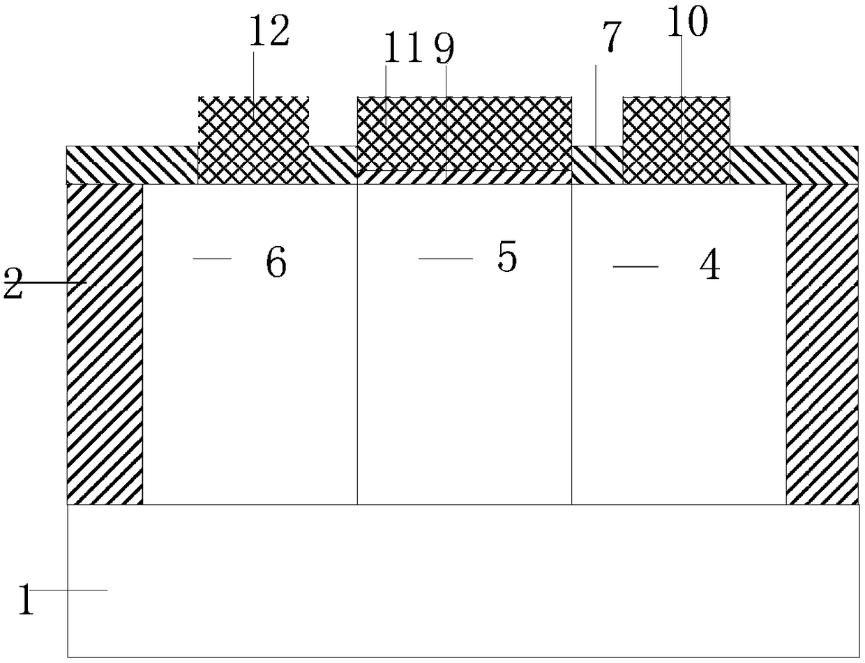
[0033] This example is for Figure 4 The structure of the off-state current suppressing TFET device is shown as an example of an N-type TFET fabricated on a P-type substrate. The N-type buried layer is in contact with the PIN structure above, and the thickness of the N-type buried layer is not less than 200nm.

[0034] The embodiment includes high-resistance P-type substrate 1, deep trench isolation 2, N-type buried layer 3, drain region 4, intrinsic region 5, source region 6, electrode isolation structure 7, thin epitaxial intrinsic region 8, gate oxide Layer 9, metal drain electrode 10, metal gate electrode 11, metal source electrode 12. The N-type buried layer is between the PIN structure and the P-type buried layer. First select the bulk silicon of the (100) crystal plane for epitaxy to obtain the required N-type buried layer. The N-type buried layer has the same doping level as the substrate and is also low-doped, and then make a PIN structure; or directly on the P Type...

Embodiment 2

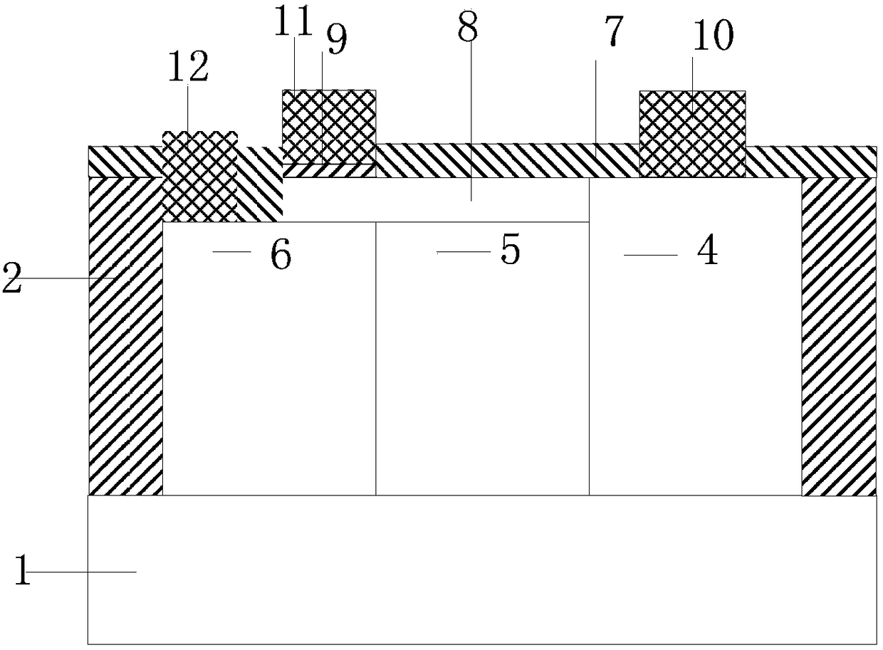
[0039] Figure 4 Although the shown N-type TFET structure can suppress the off-state current of the device, since the drain region is in contact with the buried layer, the parasitic capacitance of the drain increases, which is not conducive to the high-frequency characteristics of the device. It is modified to make it suitable for the high-frequency field, and the contact between the drain region and the buried layer of the N-type TFET is disconnected, and the area between the drain region and the buried layer is an intrinsic region, and at the same time, the buried layer is separately drawn out.

[0040] Figure 5 In order to suppress the off-state current TFET device structure applicable to the high frequency field, this embodiment is Figure 5 The shown N-type TFET device structure in which the buried layer is disconnected from the drain region, the embodiment includes a P-type substrate 1, a deep trench isolation 2, an N-type buried layer 3, a drain region 4, an intrinsic...

Embodiment 3

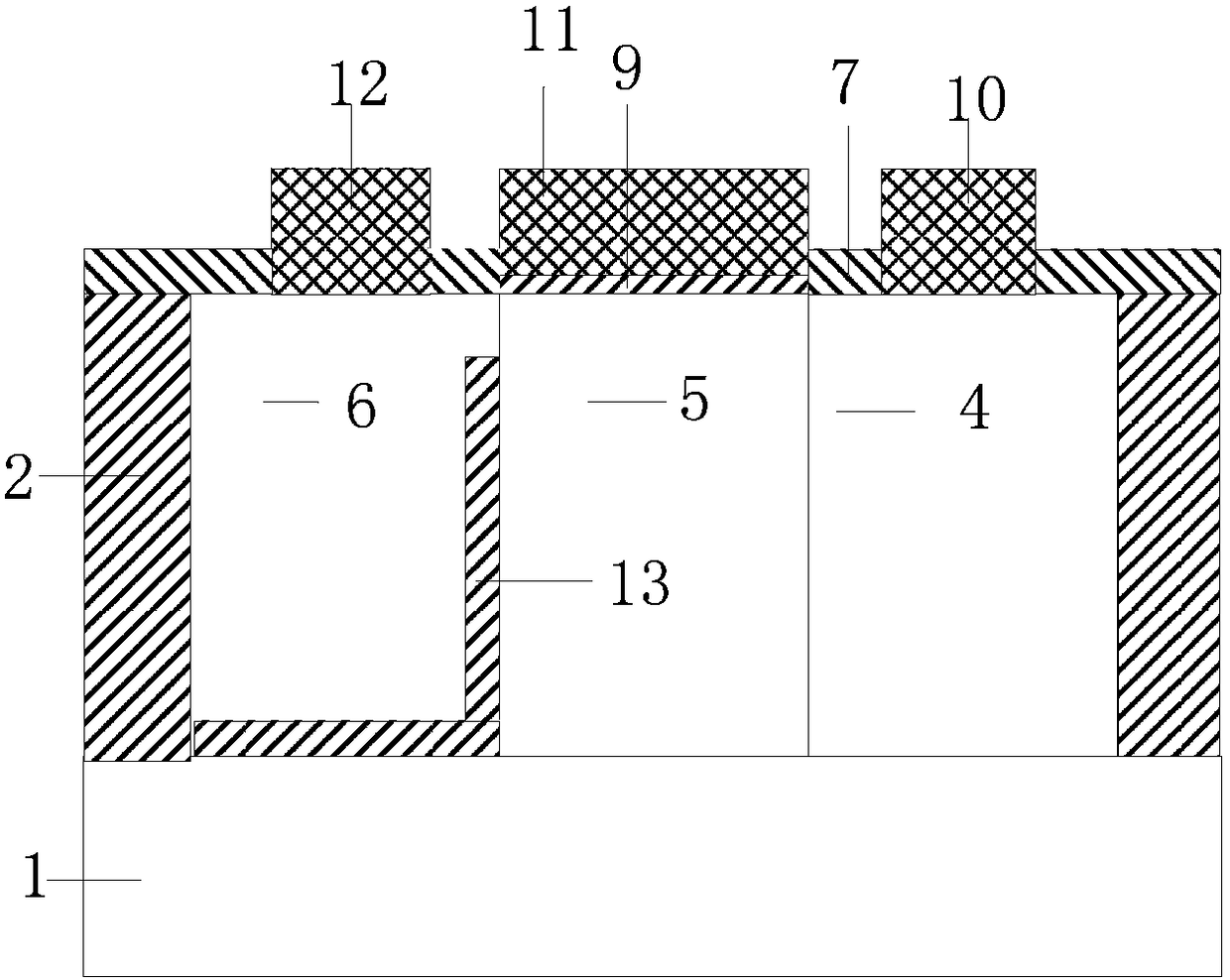
[0043] This example is for Figure 6 Shown is a lateral TFET employing the present invention to suppress off-state current. Taking an N-type TFET fabricated on a P-type substrate as an example, the N-type buried layer is in contact with the PIN structure above, and the thickness of the N-type buried layer is not less than 200nm.

[0044] The embodiment includes P-type substrate 1, deep trench isolation 2, N-type buried layer 3, drain region 4, intrinsic region 5, source region 6, electrode isolation structure 7, gate oxide layer 9, metal drain electrode 10, metal Gate electrode 11, metal source electrode 12. In the manufacturing process of the device structure in this example, the bulk silicon of the (100) crystal plane is first selected for epitaxy to obtain the required N-type buried layer. The N-type buried layer has the same doping level as the substrate and is also low-doped, and then fabricated PIN structure; or directly epitaxially sufficiently thick I layer on the P-...


PUM


Abstract

The invention discloses a tunneling field effect transistor capable of suppressing off-state current, and belongs to the field of logic devices and circuits in the field of ultra-large-scale integrated circuits. Use the short connection between the N-type drain region or the P-type source region and the N-type epitaxial layer to share a high potential, so that the N-type buried layer and the N-type source region or P-type drain region, intrinsic region, and P-type substrate The formed PN junctions are all reverse-biased, and the result is to reduce the tunneling controlled by the drain voltage in the lower part of the original device source region. The leakage current at this time is mainly the reverse bias between the N-type epitaxial layer and the N-type source region or P-type drain region. PN junction current, which effectively reduces the off-state current of the tunneling field effect transistor in the case of small size. In addition, the buried layer can be replaced with a wide bandgap material, and avoid the introduction of two-dimensional electron gas or polarized charges by the material in contact with silicon. Then the reverse bias PN junction current will be further reduced. Therefore, tunneling from the drain to the intrinsic region is suppressed, so as to reduce the off-state current of the TFET.

Description

technical field [0001] The invention belongs to the field of logic devices and circuits in the field of ultra-large-scale integrated circuits, relates to a small-sized tunneling field effect transistor, and in particular to a longitudinal tunneling TFET device which overcomes the short-channel effect and reduces off-state current. technical background [0002] With the advancement of lithography, implantation and other process technologies, the integration of chips is getting higher and higher, and the power consumption density is also increasing; moreover, the feature size of MOSFET devices is getting smaller and smaller, and the short channel effect, GIDL (gate induced Drain leakage current) becomes severe, further increasing the off-state current. Therefore, the solution to the power consumption problem directly affects the improvement of chip integration. [0003] Finding a device structure with small leakage is the most direct way to solve the static power consumption ...

Claims


Application Information

Patent Timeline
Patent Type & Authority Patents(China)
IPC IPC(8): H01L29/772H01L29/06
CPCH01L29/06H01L29/0607H01L29/772
Inventor 王向展曹建强马阳昊李竞春
Owner UNIV OF ELECTRONICS SCI & TECH OF CHINA
Why Eureka
Try Eureka