Cutting method of LED chip

A technology of LED chip and cutting method, applied in the direction of fine working devices, electrical components, circuits, etc., can solve the problems of edge chipping, ablation and twinning, and achieve the effect of avoiding ablation, easy implementation and cost reduction

Inactive Publication Date: 2015-02-11
LATTICE POWER (JIANGXI) CORP
View PDF4 Cites 24 Cited by
  • Summary
  • Abstract
  • Description
  • Claims
  • Application Information

AI Technical Summary

Problems solved by technology

[0005] The technical problem to be solved by the present invention is to provide a cutting method for LED chips, which is used to solve the problems of chipping, jumping corners, burrs, ablation and twins in the existing cutting technology.

Method used


Image

  • Cutting method of LED chip
  • Cutting method of LED chip
  • Cutting method of LED chip

Examples


Embodiment Construction

[0018] A method for cutting LED chips is provided, see FIG. 2 . Proceed as follows:

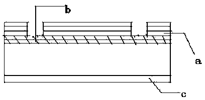
[0019] (1) Chip preparation: GaN-based semiconductor structure layer a is epitaxially grown on a silicon substrate with a thickness of 5 μm, and there are multiple layers of thick metal b and back metal c in the trench, see Figure 2 (I) ;

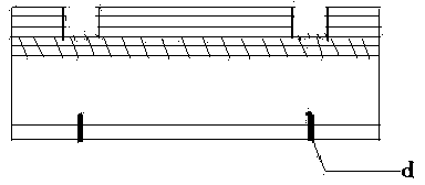
[0020] (2) Laser scribing: Paste the LED chips on the white film (model spv-224 160mm×100m) with the front facing down and the substrate facing up. It is required that there are no air bubbles between the chip and the white film. Put it on the carrier disk of the dicing machine, requiring the chip to be on the top and the film to be on the bottom. Adjust the level of the chip and determine the cutting range and laser route. Focus the 355nm ultraviolet laser emitted by the laser on the position of the dissociation groove on the upper surface of the LED chip through a corrected optical path. For scribing, adjust the laser frequency to 50-150kHz, the outp...


PUM


Abstract

The invention discloses a cutting method of an LED chip. The method comprises drawing scratches by use of laser on the back surface of the chip and performing saw cutting by use of a diamond saw blade knife, wherein the saw blade knife is an isosceles inverted triangle with a symmetrical left portion and right portion, and the included angle between a knife side surface and a horizontal line is 30 DEG to 60 DEG. The method further comprises performing overturning and film reversing on the back-cut chip and cutting the front surface of the chip along grooves to form crystal grains by use of a splinter knife. According to the invention, the problems of backside collapse, burr and the like by use of a conventional saw blade process are solved, the problem of ablation brought by laser cutting is avoided, and the method is simple to operate and easy to realize.

Description

technical field [0001] The invention relates to the field of semiconductor light emitting diodes, in particular to a method for cutting LED chips. Background technique [0002] In the LED chip manufacturing process, dicing is to divide the whole chip into single grains that meet the required size, which is an indispensable process in the semiconductor light-emitting diode chip manufacturing process. For LED chips, there are currently two cutting processes: saw blade cutting and laser cutting. The traditional and most widely used cutting method in the industry is saw blade cutting. [0003] Saw blade cutting is to use a high-speed rotating saw blade to completely saw the chip into a single grain according to the set program. Saw blade cutting technology is quite mature, and it is still the mainstream technology for cutting chips based on gallium arsenide, silicon, and gallium phosphide. But there is a problem with this method: some semiconductor materials are very brittle,...

Claims


Application Information

Patent Timeline
Patent Type & Authority Applications(China)
IPC IPC(8): H01L33/00H01L21/78
CPCH01L33/0095B28D5/0011H01L21/78
Inventor 刘乐功封波邓彪孙钱赵汉民
Owner LATTICE POWER (JIANGXI) CORP
Why Eureka
Try Eureka