Array substrate, production method thereof and display device

A technology of an array substrate and a manufacturing method, applied in the display field, can solve the problems affecting the conduction characteristics of TFT, surface roughness, etc., and achieve the effects of ensuring display quality, repairing damage, and improving electrical characteristics

Active Publication Date: 2015-02-18
BOE TECH GRP CO LTD +1
View PDF5 Cites 25 Cited by
  • Summary
  • Abstract
  • Description
  • Claims
  • Application Information

AI Technical Summary

Problems solved by technology

[0008] The invention provides an array substrate, its manufacturing method, and a display device, which are used to solve the problem that the via etching process in the insulating structure will cause the surface of the active layer below to be rough, thereby affecting the conduction characteristics of the entire TFT

Method used


Image

  • Array substrate, production method thereof and display device
  • Array substrate, production method thereof and display device
  • Array substrate, production method thereof and display device

Examples


Embodiment Construction

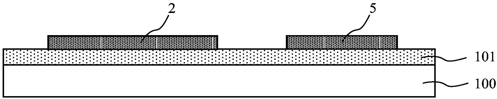
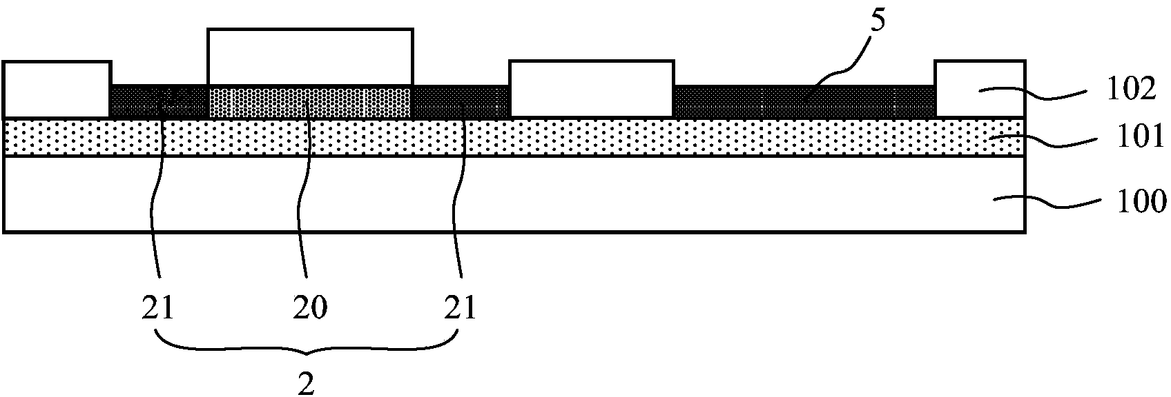
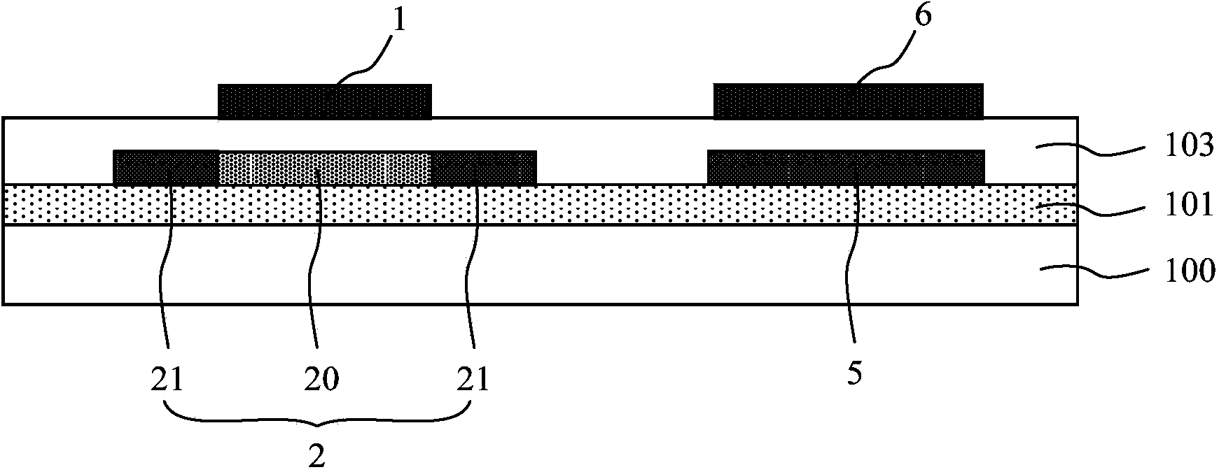
[0027] In the manufacturing process of the array substrate, the electrical connection between different conductive layers is generally completed by making insulating layer via holes, that is, different conductive layers are electrically contacted through the insulating layer via holes. When the array substrate includes thin film transistors, the gold half-electric contact between the source electrode, the drain electrode and the active layer pattern (specifically referring to the electrical contact between the source and drain metal and the semiconductor active layer) is realized through the insulating layer via holes, forming an insulating layer. In the etching process of the layer via hole, in order to ensure that the via hole is etched completely without residue, the active layer at the via hole will also be etched, resulting in rough surface of the active layer at the via hole, and the subsequent source When the electrode and the drain electrode are in contact with the acti...


PUM


Abstract

The invention relates to the technical field of display, and discloses an array substrate, a production method thereof and a display device. The array substrate comprises a thin film transistor, and a source electrode and a drain electrode of the thin film transistor are located over an active layer pattern and electrically contacts with the active layer pattern through via holes in an insulation structure. Before the source electrode and the drain electrode are produced, the active layer pattern is subjected to ion implantation through the via holes in the insulation layer to form an ion implantation region, so that damage to the surface of the active layer pattern due to the etching process for forming the via holes can be repaired, electric metal-semiconductor contact performance of the source electrode and the drain electrode with the active layer pattern is improved, electrical properties of the thin film transistor are improved, and display quality of the display device is guaranteed.

Description

technical field [0001] The present invention relates to the field of display technology, in particular to an array substrate, a manufacturing method thereof, and a display device. Background technique [0002] Active matrix organic light emitting diode (Active Matrix Organic Light Emitting Diode, referred to as AMOLED) display device is a new type of flat panel display device. Therefore, the viewing angle and contrast of AMOLED display devices are better than liquid crystal displays, and have the advantages of small size, light weight and low power consumption. At the same time, since the AMOLED display device uses a low DC driving thin-film transistor (Thin-Film Transistor, TFT for short) to transmit the pixel voltage to the OLED for display, it has the advantage of fast response. AMOLED display devices can also work over a wider temperature range and are less expensive to produce. [0003] TFT can be divided into polysilicon (p-Si) TFT and amorphous silicon (a-Si) TFT, t...

Claims


Application Information

Patent Timeline
Patent Type & Authority Applications(China)
IPC IPC(8): H01L21/77H01L27/12
CPCH01L27/1214H01L27/1259H10K59/12H01L29/78618H01L27/127H01L27/1255H10K59/1201H10K59/1213H10K59/124H10K59/131H10K59/1216H01L21/77H01L27/12H01L27/124H01L27/1288
Inventor 谢振宇
Owner BOE TECH GRP CO LTD
Why Eureka
Try Eureka