Method for manufacturing substrate of LED thin film chip and structure of substrate

A thin-film chip and substrate technology, which is applied in the field of preparation of LED thin-film chip substrates

Active Publication Date: 2015-02-18
NANCHANG UNIV +1
View PDF6 Cites 2 Cited by
  • Summary
  • Abstract
  • Description
  • Claims
  • Application Information

AI Technical Summary

Problems solved by technology

[0007] The first purpose of the present invention is to provide a method for preparing a LED thin film chip substrate with high reliability, which can solve the problem of the gap between the substrate support material and the bonding metal. The problem of poor adhesion between the substrates and the problem of substrate bowing due to residual stress
[0008] The second object of the present invention is to provide a LED thin film chip substrate structure, which is used to solve the problem of poor adhesion between the substrate support material and the bonding metal and the problem of substrate bowing due to residual stresses

Method used


Image

  • Method for manufacturing substrate of LED thin film chip and structure of substrate
  • Method for manufacturing substrate of LED thin film chip and structure of substrate
  • Method for manufacturing substrate of LED thin film chip and structure of substrate

Examples


Embodiment 1

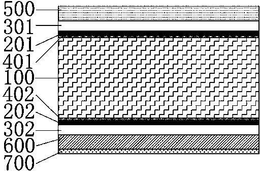
[0074] figure 1 and figure 2 ~7 describes the preparation method of a kind of LED thin film chip substrate of embodiment 1 of the present invention, and this preparation method comprises the following steps:

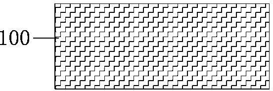
[0075] A, prepare a substrate support body 100, such as figure 2 shown, and its surface was cleaned; in this embodiment, a Si wafer with good thermal and electrical conductivity was selected as the substrate support, and its thickness was 250 μm.

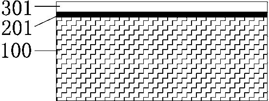
[0076] B. Forming the first alloy preparation layer 201 and the first substrate protection layer 301 sequentially on the front surface of the substrate support 100 by means of electron beam evaporation or sputtering, as shown in FIG. 3 ;

[0077] C. Forming a second alloy preparation layer 202 and a second substrate protection layer 302 sequentially on the reverse side of the substrate support 100, as shown in FIG. 4 ;

[0078] The materials of the second alloy preparation layer 201 and the second alloy preparation layer...

Embodiment 2

[0109] The difference from Embodiment 1 is that in Embodiment 2, the first substrate protection layer 301 and the second substrate protection layer 302 are respectively formed on the front surface of the substrate support 100 after the alloying process is completed. and the opposite side, while the structure of a LED thin film chip substrate obtained in Example 2 is exactly the same as that in Example 1.

[0110] A kind of preparation method of LED thin film chip substrate provided in embodiment 2, comprises the following steps:

[0111] A. Provide a substrate support body 100 with a clean surface;

[0112] B. A first alloy preparation layer 201 is sequentially formed on the front surface of the substrate support, and a second alloy preparation layer 202 is sequentially formed on the reverse surface of the substrate support, as shown in FIG. 8 ;

[0113] C. Carry out alloying, make the first alloy preparation layer 201, the second alloy preparation layer 201 and the subs...


PUM

PropertyMeasurementUnit
thicknessaaaaaaaaaa
thicknessaaaaaaaaaa
thicknessaaaaaaaaaa

Abstract

The invention provides a method for manufacturing a substrate of an LED thin film chip and a structure of the substrate. The method and the structure have the advantages that an alloy preparation layer is manufactured on the surface of a substrate support material, a binary blended layer is formed by alloy and the substrate support material, and accordingly a semiconductor material and metal interface which is high in reliability can be obtained; a stress modulation layer is formed below the substrate support material, and a thermal expansion coefficient of the stress modulation layer can be adjusted, so that stress which is exerted to the substrate by an LED thin film positioned on the upper side of the substrate can be balanced, and the problem of bending of existing substrates can be solved; the structural strength and the thickness of the stress modulation layer can be adjusted, so that the bending resistance of the can be improved.

Description

technical field [0001] The invention belongs to the technical field of semiconductor optoelectronic device manufacturing, and in particular relates to a method for preparing an LED thin film chip substrate and a structure thereof. Background technique [0002] In the early stage of LED development, the chip structure was mostly based on the same-side electrode structure on the growth substrate. With the gradual improvement of LED luminous efficiency, the application range is wider and wider. LED chips have gradually developed from traditional low-power chips used for indication and display to high-power chips that can be used in lighting and other applications. Due to many problems in the same-side structure, such as high working voltage, current congestion, easy current saturation, low pn junction utilization, poor current expansion, etc., lighting power chips that require good heat dissipation structure and current expansion need to use A more advanced chip with a vertica...

Claims


Application Information

Patent Timeline
Patent Type & Authority Applications(China)
IPC IPC(8): H01L33/00
CPCH01L33/44H01L33/48H01L2933/0025
Inventor 王光绪刘军林陶喜霞江风益
Owner NANCHANG UNIV
Why Eureka
Try Eureka