LED structure and manufacturing method thereof
A technology of LED structure and manufacturing method, applied in electrical components, circuits, semiconductor devices, etc., can solve the problems of increased production costs, limited space for brightness improvement, and no improvement in luminous efficiency, and achieves the effect of reducing manufacturing costs and costs.
- Summary
- Abstract
- Description
- Claims
- Application Information
AI Technical Summary
Problems solved by technology
Method used
Image

Examples
Embodiment 1
[0083] Figure 1 to Figure 8 A schematic diagram of a cross-sectional structure in the process of fabricating the patterned substrate provided in this embodiment, Figure 17 The flow chart of the method for fabricating the patterned substrate of the present embodiment is combined below Figure 17 and Figures 1 to 8 The method for forming the patterned substrate according to the specific embodiment of the present invention will be described in detail.
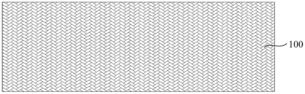
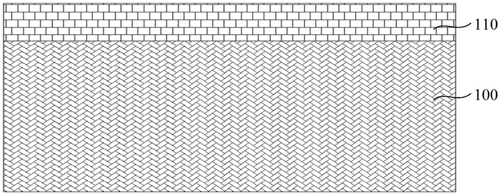
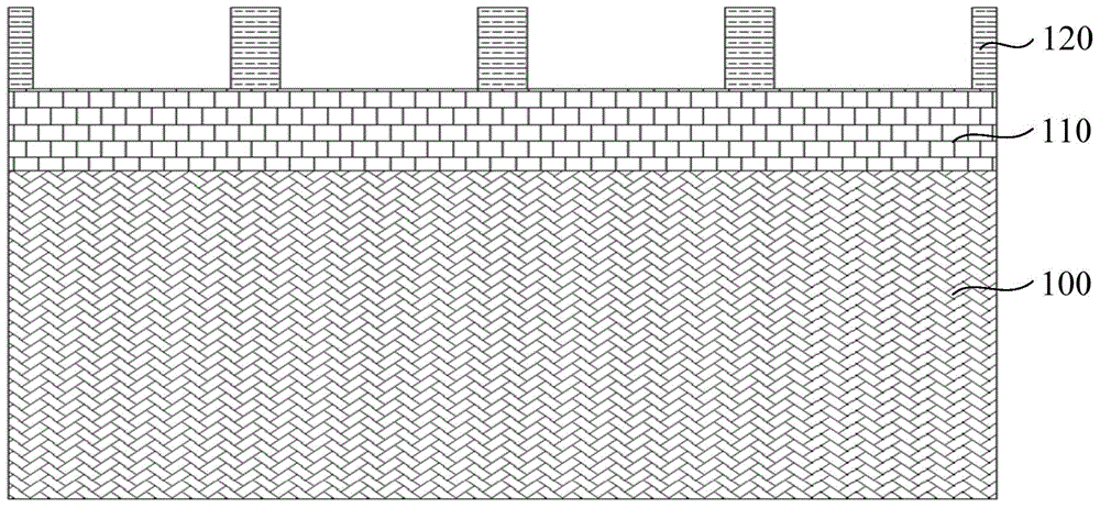
[0084] like figure 1 As shown, step S11 is performed to provide an original substrate 100, and the original substrate 100 may be a silicon carbide (SiC) original substrate, a sapphire (Al2O3) original substrate or a silicon original substrate. In this embodiment, a sapphire substrate is used.
[0085] like figure 2As shown, step S12 is performed to form a first mask layer 110 on the original substrate 100 through processes such as evaporation, sputtering, spray coating, PECVD or LPCVD. Preferably, a first mask layer 110 ...
Embodiment 2
[0102] like Figure 9 As shown, the difference between the patterned substrate provided in this embodiment and the patterned substrate provided in Embodiment 1 is that the second pattern structure 102 is a cone-shaped structure.
[0103] In the method for fabricating the patterned substrate of the LED structure provided in this embodiment, on the basis of the first embodiment, additional etching is performed for a predetermined time (or the etching time in step S17 is directly extended). The second pattern structure 102 is transformed from a mesa-like structure to a cone-like structure. The specific process parameters can be obtained through a limited number of experiments according to the characteristics of the machine and the thickness and corrosion resistance of the silicon dioxide to be formed.
[0104] The positional relationship between the original substrate 100 and the first pattern structure 101 , the second pattern structure 102 , and the third pattern structure 103...
Embodiment 3
[0106] like Figure 11 As shown, the difference between the patterned substrate provided in this embodiment and the patterned substrate provided in Embodiments 1 and 2 is that the first pattern structure 101 is a rectangular ring structure and the rectangular ring structure is along the The longitudinal section of each side in the width direction (section perpendicular to the surface of the original substrate) is triangular, and several second pattern structures 102 and third pattern structures 103 are not formed.
[0107] like Figure 18 As shown, the manufacturing method of the patterned substrate of the LED structure provided by this embodiment includes the following steps:
[0108] Step S31, providing an original substrate 100;
[0109] Step S32, forming a first mask layer 110 on the original substrate 100;
[0110] Step S33, a patterned photoresist layer 120 is formed on the first mask layer 110 by a photolithography process, and the patterned photoresist layer 120 is ...
PUM
 Abstract
Description
Claims
Application Information
 - R&D
- Intellectual Property
- Life Sciences
- Materials
- Tech Scout
- Unparalleled Data Quality
- Higher Quality Content
- 60% Fewer Hallucinations
Browse by: Latest US Patents, China's latest patents, Technical Efficacy Thesaurus, Application Domain, Technology Topic, Popular Technical Reports.
© 2025 PatSnap. All rights reserved.Legal|Privacy policy|Modern Slavery Act Transparency Statement|Sitemap|About US| Contact US: help@patsnap.com