Method of forming flip-chip semiconductor encapsulation device

A flip-chip and semiconductor technology, which is applied in semiconductor devices, semiconductor/solid-state device manufacturing, semiconductor/solid-state device components, etc., can solve problems such as residual stress, delamination, and difficulty in dissipating heat from chips to achieve simple structure , Strong applicability, strong heat dissipation effect

Inactive Publication Date: 2015-03-04
NANTONG FUJITSU MICROELECTRONICS
View PDF7 Cites 5 Cited by
  • Summary
  • Abstract
  • Description
  • Claims
  • Application Information

AI Technical Summary

Problems solved by technology

[0004] 1. In the traditional semiconductor chip flip-chip packaging structure, the chip is suspended on the carrier board, and it is difficult for the suspended chip to dissipate heat sufficiently, which in turn affects the electrothermal performance and reliability of the final product
[0005] 2. In the traditional semiconductor lead frame package, most of the heat generated by the chip is conducted through the metal plate in the package. In order to meet the high heat dissipation requirements, the area of ​​the carrier plate is increased. On the one hand, it will be affected by the difference in thermal expansion rate between different materials. It is easy to produce reliability problems such as stress residue and delamination; on the other hand, it does not meet the development requirements of the trend of semiconductor packages becoming thinner and smaller
[0006] 3. The traditional semiconductor packaging structure also improves the heat dissipation effect by selecting high-conductivity thermoplastic sealing materials. In addition to its own cost and price, high-conductivity thermoplastic sealing materials also put forward higher requirements for the control of the product plastic packaging process. And the heat dissipation effect is not obvious

Method used


Image

  • Method of forming flip-chip semiconductor encapsulation device
  • Method of forming flip-chip semiconductor encapsulation device
  • Method of forming flip-chip semiconductor encapsulation device

Examples


Embodiment Construction

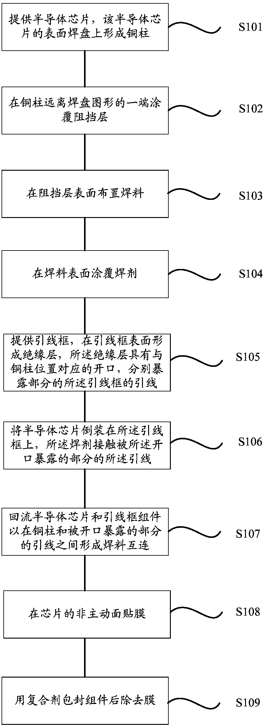
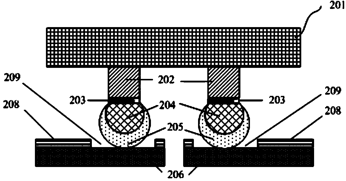
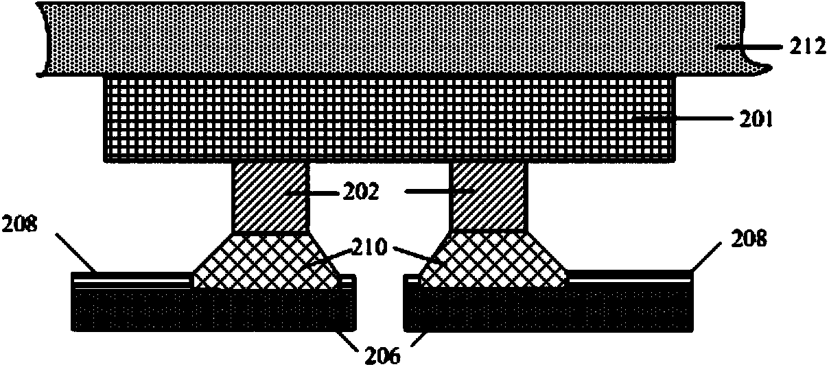
[0044] In order to make the above objects, features and advantages of the present invention more comprehensible, the specific implementation manners of the present invention will be further described in detail below in conjunction with the accompanying drawings.

[0045] In the following description, specific details are set forth in order to provide a thorough understanding of the invention. However, the present invention can be implemented in many other ways than those described here, and those skilled in the art can make similar extensions without departing from the connotation of the present invention. Accordingly, the invention is not limited to the specific implementations disclosed below.

[0046] In view of the above drawbacks, the present invention provides a method for forming a flip-chip semiconductor package.

[0047] A detailed description will be given below in conjunction with the accompanying drawings. For convenience of description, only a part of the lead f...


PUM

PropertyMeasurementUnit
heightaaaaaaaaaa
diameteraaaaaaaaaa
heightaaaaaaaaaa

Abstract

The invention discloses a method of forming a flip-chip semiconductor encapsulation device. The method includes the following steps that: copper columns are formed on a pad pattern of a semiconductor chip, and one end of each copper column, which is far away from the pad pattern, is plated with a barrier layer, and a predetermined amount of solder is distributed on the barrier layers, and the solder is coated with soldering flux; lead frames are provided, and the surfaces of the lead frames are plated with insulating layers, and openings corresponding to the positions of the copper columns, are formed in the insulating layers and expose a part of leads of the lead frames respectively; the semiconductor chip is mounted on the lead frames in a flip manner, and the solder contacts with the exposed leads; when refluxing is performed, the solder is melt, and solder interconnection structures are formed between the copper columns and the exposed leads by means of the soldering flux; and after the refluxing, a film is attached to a non-active surface of the chip, and then, encapsulation is performed, and the film is removed, and therefore, the flip-chip semiconductor encapsulation device can be formed. According to the method, the non-active surface of the chip is not covered with the encapsulation material, so that the formed flip-chip semiconductor device can have an excellent heat dissipation effect.

Description

technical field [0001] The invention relates to the technical field of semiconductors, in particular to a method for forming a flip-chip semiconductor package on a lead frame. Background technique [0002] Over time, semiconductor packages are becoming smaller and more concentrated and manufactured in a variety of shapes. Semiconductor packages are typically classified into a wire bonding type or a flip chip bonding type according to a connection method. The wire-bonding type of package uses conductive bonding wires to connect the electrodes of the semiconductor chip to the lead frame, while the flip-chip type of package uses conductive bumps placed on the electrode pads of the semiconductor chip, Connecting terminals to connect semiconductors to leads or to connect semiconductor chips directly to circuit boards. Flip-chip bonding type packages have a shorter electrical connection path than metal bonding type packages, thus providing excellent thermal and electrical charac...

Claims


Application Information

Patent Timeline
Patent Type & Authority Applications(China)
IPC IPC(8): H01L21/60H01L21/56H01L21/48H01L23/31
CPCH01L24/81H01L2224/16245H01L2224/16058H01L2924/181H01L2924/00
Inventor 石磊
Owner NANTONG FUJITSU MICROELECTRONICS
Why Eureka
Try Eureka