Multi-junction solar cell based on semiconductor quantum dot, and manufacturing method thereof

A technology of solar cells and production methods, applied in the field of solar cells, can solve problems such as high cost

Active Publication Date: 2015-03-04
SUZHOU JUZHEN PHOTOELECTRIC
View PDF5 Cites 10 Cited by
  • Summary
  • Abstract
  • Description
  • Claims
  • Application Information

AI Technical Summary

Problems solved by technology

[0006] For this reason, the technical problem to be solved by the present invention is that traditional multi-junction III-V semiconductor solar cells are generally three pairs of p-n junctions formed by epitaxial growth of GaInAs and GaInP semicondu

Method used


Image

  • Multi-junction solar cell based on semiconductor quantum dot, and manufacturing method thereof
  • Multi-junction solar cell based on semiconductor quantum dot, and manufacturing method thereof
  • Multi-junction solar cell based on semiconductor quantum dot, and manufacturing method thereof

Examples


Embodiment 1

[0033] This embodiment provides a method for manufacturing a multi-junction solar cell based on semiconductor quantum dots,

[0034] Include the following steps:

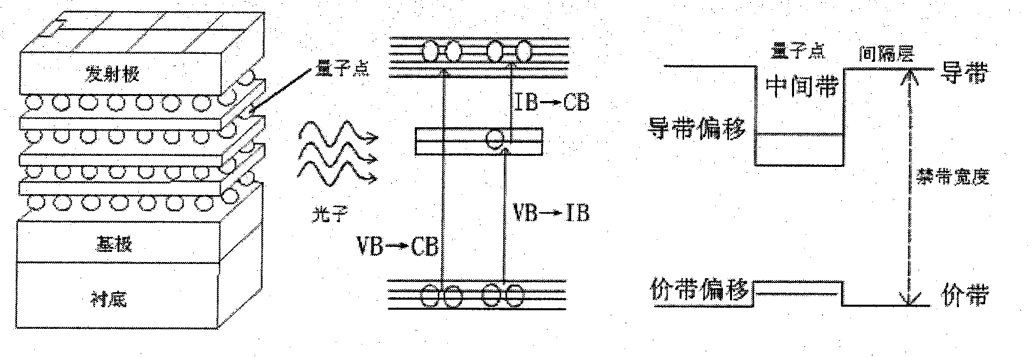
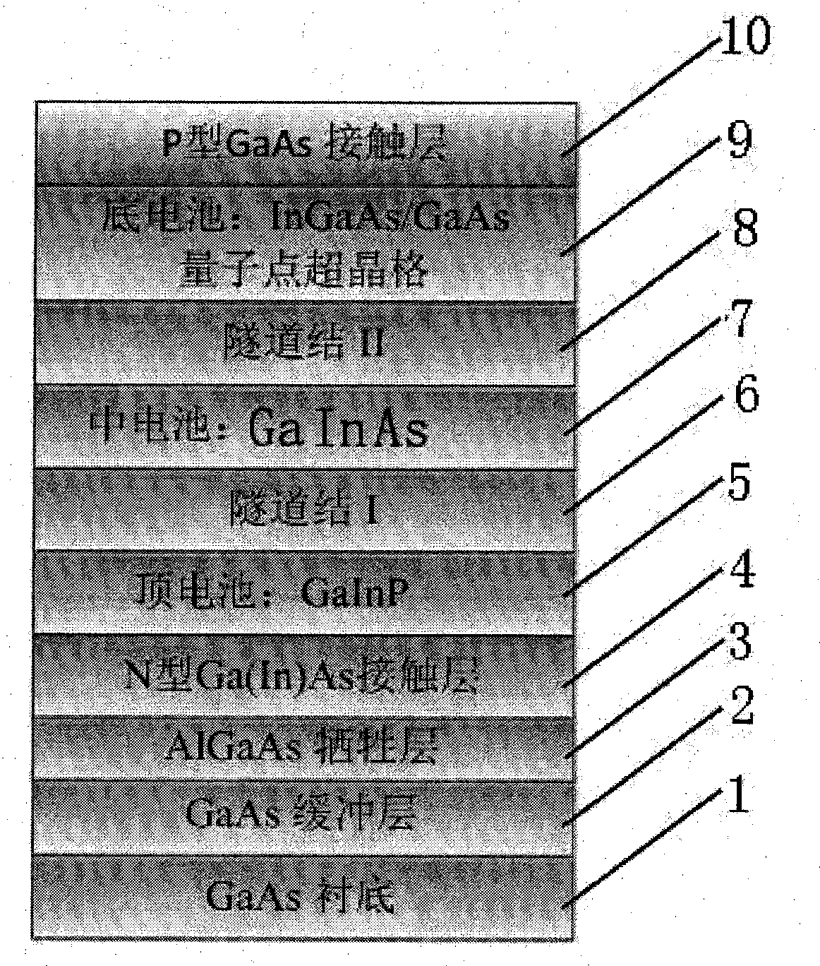
[0035] Step S1: epitaxially grow the buffer layer 2, the sacrificial layer 3 and the solar cell layer on the GaAs substrate 1 in order to produce a solar cell epitaxial wafer. The solar cell layer includes an N-type contact layer 4, a GaInP top cell 5, a tunnel junction I6, and GaInAs Middle cell 7, tunnel junction II8, InGaAs / GaAs quantum dot bottom cell 9 and P-type contact layer 10, the band gap of GaInP top cell 5 is 1.80-1.92eV, and the band gap of GaInAs middle cell 7 is 1.38-1.42eV , the forbidden band width of the InGaAs / GaAs quantum dot bottom cell 9 is 1.0-1.3eV. Specifically, the InGaAs / GaAs quantum dot bottom cell 9 includes a quantum dot superlattice structure and a base and an emitter that are separately arranged on both sides of the quantum dot superlattice structure, and the quantum dot superlattice...

Embodiment 2

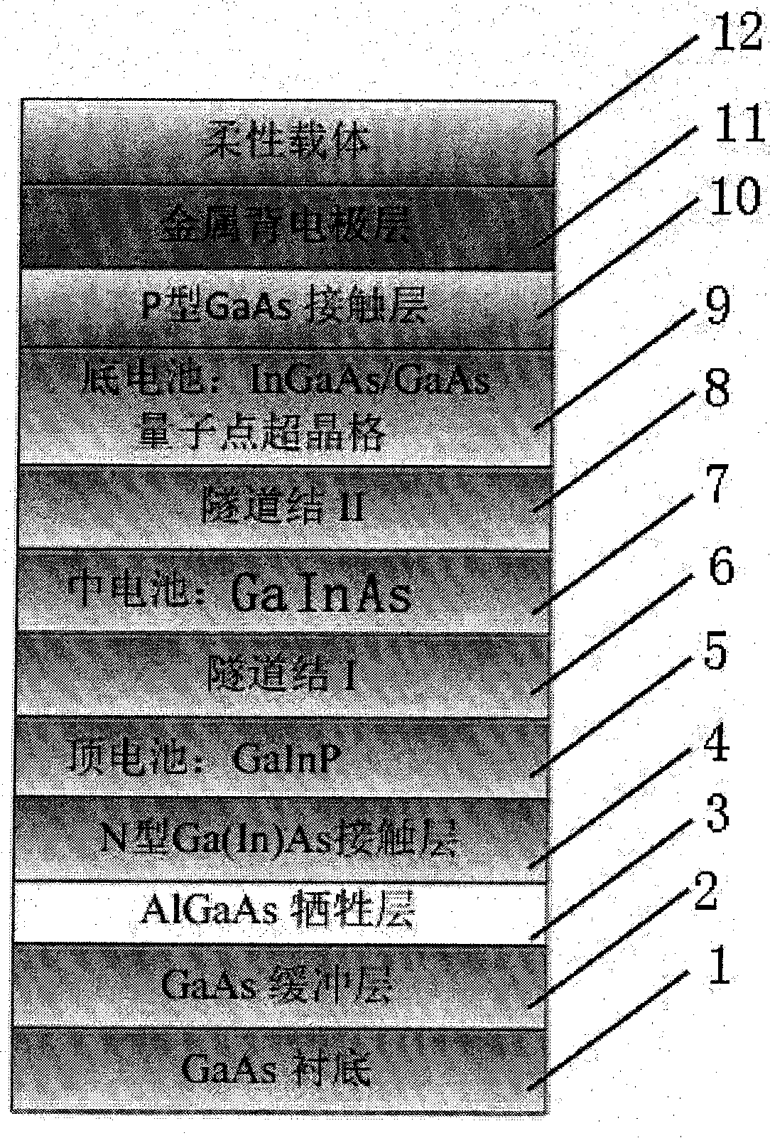
[0049] Such as Figure 5 As shown, this embodiment provides a multi-junction solar cell based on semiconductor quantum dots, including a control chip and a plurality of series and / or parallel battery cells connected to the control chip, characterized in that the battery cells are from top to The bottom includes metal back electrode layer 11, P-type contact layer 10, InGaAs / GaAs quantum dot bottom cell 9, tunnel junction II8, GaInAs middle cell 7, tunnel junction I6, GaInP top cell 5, and N-type contact layer 4. It also includes an anti-reflection film 14 and an upper electrode 13 arranged on the N-type GaInAs contact layer.

[0050] Specifically, the InGaAs / GaAs quantum dot bottom cell 9 includes a quantum dot superlattice structure and a base and an emitter that are separately arranged on both sides of the quantum dot superlattice structure, and the quantum dot superlattice structure includes at least one layer of In x Ga 1-x As quantum dot layer, and set in In x Ga 1-x G...


PUM

PropertyMeasurementUnit
Thicknessaaaaaaaaaa
Lattice constantaaaaaaaaaa
Thicknessaaaaaaaaaa

Abstract

The invention provides a multi-junction solar cell based on a semiconductor quantum dot, and a manufacturing method thereof. The method comprises the following steps: successively growing a buffer layer, a sacrifice layer and a solar cell layer in an epitaxial mode on a GaAs substrate, and manufacturing an epitaxial wafer, wherein the solar cell layer comprises an N-type contact layer, a GaInP top cell, a tunnel junction I, a GaInAs intermediate cell, a tunnel junction II, an InGaAs/GaAs quantum dot bottom cell and a P-type contact layer, the forbidden band width of the GaInP top cell is 1.80 to 1.92 eV, the forbidden band width of the GaInAs intermediate cell is 1.38 to 1.42 eV, and the forbidden band width of the InGaAs/GaAs quantum dot bottom cell is 1.0 to 1.3 eV; and manufacturing the multi-junction solar cell based on the semiconductor quantum dot by use of the epitaxial wafer. Compared to a conventional multi-junction solar cell, the multi-junction solar cell based on the semiconductor quantum dot has the following advantages: the device structure and the concentrating system are simple, the flexibility is high, the manufacturing process is simple, and the production cost is low.

Description

technical field [0001] The invention relates to the technical field of solar cells, in particular to a multi-junction solar cell based on semiconductor quantum dots and a manufacturing method thereof. Background technique [0002] Traditional energy represented by coal, oil and natural gas will cause serious environmental pollution. Therefore, renewable clean energy represented by the solar photovoltaic industry has received widespread attention and achieved rapid development. The conversion efficiencies of monocrystalline silicon and polycrystalline silicon solar cell modules, which currently dominate the photovoltaic market, are around 18% and 15%, respectively. Since silicon materials and gallium arsenide (GaAs) are indirect bandgap and direct bandgap semiconductor materials respectively, the theoretical photoelectric conversion efficiency (23%) of silicon solar cells is much lower than that of gallium arsenide solar cells, among which single-junction gallium arsenide Th...

Claims


Application Information

Patent Timeline
IPC IPC(8): H01L31/18H01L31/0352H01L31/0687H01L31/0693
CPCH01L31/035218H01L31/0687H01L31/0693H01L31/18Y02E10/544Y02P70/50
Inventor 杨晓杰叶继春刘凤全
Owner SUZHOU JUZHEN PHOTOELECTRIC
Why Eureka
Try Eureka