LED (Light Emitting Diode) chip and manufacturing method thereof

An LED chip and manufacturing method technology, applied in electrical components, circuits, semiconductor devices, etc., can solve the problems of large current density and light emitting angle, and achieve the effects of increasing light efficiency, reducing current accumulation, and increasing light emitting angle.

Active Publication Date: 2015-03-04
XIANGNENG HUALEI OPTOELECTRONICS
View PDF5 Cites 10 Cited by
  • Summary
  • Abstract
  • Description
  • Claims
  • Application Information

AI Technical Summary

Problems solved by technology

Although this can reduce the current ratio under the electrodes, the current density between the N and P electrodes is higher than the current density in the edge area and the problem of the light output angle in the area where the current density is concentrated

Method used


Image

  • LED (Light Emitting Diode) chip and manufacturing method thereof
  • LED (Light Emitting Diode) chip and manufacturing method thereof
  • LED (Light Emitting Diode) chip and manufacturing method thereof

Examples


Embodiment 1

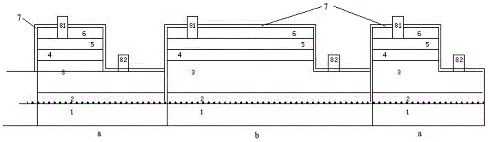
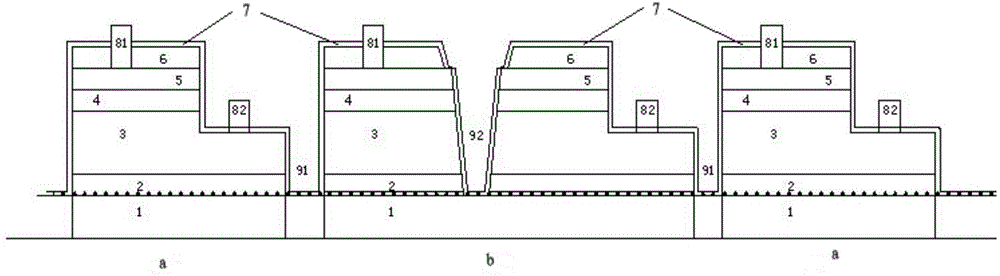
[0047] Such as figure 2 with image 3 As shown, this embodiment provides an LED chip, including: a PSS substrate 1, a buffer layer 2, an N-type semiconductor layer 3, a light-emitting layer 4, a P-type semiconductor layer 5, a transparent conductive layer 6 and Protective layer 7.

[0048] The PSS substrate 1 in the present invention is a patterned sapphire substrate. The transparent conductive layer 6 is an indium tin oxide film. The protective layer 7 is a protective layer made of silicon dioxide. Of course, the material of the protective layer is not specifically limited here.

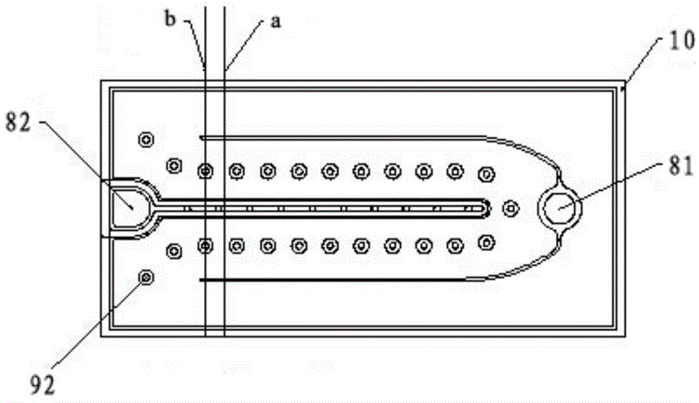
[0049] A P electrode 81 is provided on the transparent conductive layer 6, and the P electrode 81 extends axially to penetrate the protective layer 7, and an N electrode 82 is provided on the N-type semiconductor layer 3. The P electrode 81 and the N electrode 82 are both reflective electrode structures Here, the reflective electrode structure is a nickel / aluminum structure or a nickel / silver structur...

Embodiment 2

[0070] Such as figure 2 with image 3 As shown, this embodiment provides an LED chip, including: a PSS substrate 1, a buffer layer 2, an N-type semiconductor layer 3, a light-emitting layer 4, a P-type semiconductor layer 5, a transparent conductive layer 6 and Protective layer 7.

[0071] The PSS substrate 1 in the present invention is a patterned sapphire substrate. The transparent conductive layer 6 is an indium tin oxide film. The protective layer 7 is a protective layer made of silicon dioxide. Of course, the material of the protective layer is not specifically limited here.

[0072] A P electrode 81 is provided on the transparent conductive layer 6, the P electrode 81 extends axially to penetrate the protective layer 7, and an N electrode 82 is provided on the N-type semiconductor layer 3. The P electrode 81 and the N electrode 82 are both reflective electrodes Structure, the reflective electrode structure here is a nickel / aluminum structure or a nickel / silver structure, t...

Embodiment 3

[0093] Such as figure 2 with image 3 As shown, this embodiment provides an LED chip, including: a PSS substrate 1, a buffer layer 2, an N-type semiconductor layer 3, a light-emitting layer 4, a P-type semiconductor layer 5, a transparent conductive layer 6 and Protective layer 7.

[0094] The PSS substrate 1 in the present invention is a patterned sapphire substrate. The transparent conductive layer 6 is an indium tin oxide film. The protective layer 7 is a protective layer made of silicon dioxide. Of course, the material of the protective layer is not specifically limited here.

[0095] A P electrode 81 is provided on the transparent conductive layer 6, and the P electrode 81 extends axially to penetrate the protective layer 7, and an N electrode 82 is provided on the N-type semiconductor layer 3. The P electrode 81 and the N electrode 82 are both reflective electrode structures Here, the reflective electrode structure is a nickel / aluminum structure or a nickel / silver structur...


PUM


Abstract

The invention discloses an LED (Light Emitting Diode) chip. The LED chip comprises a PSS (Patterned Sapphire Substrate), a buffer layer, an N type semiconductor layer, a luminous layer, a P type semiconductor layer, a transparent conducting layer and a protection layer which are sequentially arranged along the axial direction. The invention also provides an LED chip manufacturing method. According to the LED chip, a groove which leads to the PSS is arranged between an N electrode and a P electrode of the chip, current insulating layers are formed between the N electrode and the P electrode due to the groove, and accordingly gathering of currents between the N electrode and the P electrode is blocked, the LED chip plays a role in blocking the currents, meanwhile the currents transversely expand to other areas, gathering of the currents is reduced, diffusion of the currents is uniform, the thermal stability of the LED chip is improved, and the service life of a device can be prolonged.

Description

Technical field [0001] The present invention relates to the field of semiconductor technology, in particular, to a new type of light emitting diode chip and a manufacturing method thereof. Background technique [0002] Light-Emitting Diode (LED for short) is a semiconductor electronic device that converts electrical energy into light energy. When current flows, electrons and holes recombine in it to emit monochromatic light. LED lighting has been widely used in home, decoration, office, signs and even street lamps. [0003] At present, the luminous efficiency of light-emitting diode (LED) chips is mainly divided into internal quantum efficiency and external quantum efficiency. Due to the refractive index of the GaN material itself, the light output angle is small. At present, the structure of the light-emitting diode (LED) chip has a formal structure Due to the current accumulation effect of the LED chip, the vertical structure and flip-chip welding structure, the front-mounted s...

Claims


Application Information

Patent Timeline
Patent Type & Authority Applications(China)
IPC IPC(8): H01L33/22H01L33/10H01L33/20H01L33/40H01L33/44H01L33/00
CPCH01L33/005H01L33/10H01L33/20H01L33/22H01L33/405H01L33/42H01L33/46H01L2933/0008
Inventor 何鹏付宏威
Owner XIANGNENG HUALEI OPTOELECTRONICS
Why Eureka
Try Eureka