Highly integrated grooved insulated gate tunneling bipolar enhancement transistor and its manufacturing method

An insulated gate and transistor technology, which is applied in the field of highly integrated groove insulated gate tunneling bipolar enhanced transistors and their manufacturing, can solve the problems of small forward conduction current, increased process difficulty, deterioration of device switching characteristics, etc., and achieves high integration degree, saving chip area, and the effect of excellent switching characteristics

Inactive Publication Date: 2017-04-26
SHENYANG POLYTECHNIC UNIV
View PDF4 Cites 0 Cited by
  • Summary
  • Abstract
  • Description
  • Claims
  • Application Information

AI Technical Summary

Problems solved by technology

Although the degradation of this device performance can be alleviated by improving the structure of the gate electrode, when the device size is further reduced, the switching characteristics of the device will continue to deteriorate
[0005] Compared with MOSFETs, tunneling field-effect transistors (TFETs) proposed in recent years have improved their average subthreshold swing, but their forward conduction current is too small. Materials with a narrower band gap to generate the tunneling part of TFETs can increase the tunneling probability to improve switching characteristics, but increase the difficulty of the process
Using a high dielectric constant insulating material as the insulating dielectric layer between the gate and the substrate can improve the control ability of the gate to the electric field distribution of the channel, but it cannot essentially increase the tunneling probability of silicon materials. Therefore, for TFETs The forward conduction characteristic of the improvement is very limited

Method used


Image

  • Highly integrated grooved insulated gate tunneling bipolar enhancement transistor and its manufacturing method
  • Highly integrated grooved insulated gate tunneling bipolar enhancement transistor and its manufacturing method
  • Highly integrated grooved insulated gate tunneling bipolar enhancement transistor and its manufacturing method

Examples


Embodiment Construction

[0048] Below in conjunction with accompanying drawing, the present invention will be further described:

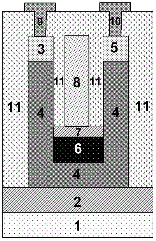
[0049] Such as figure 1 It is a schematic diagram of a two-dimensional structure of a highly integrated grooved insulated gate tunneling bipolar enhancement transistor formed on an SOI substrate according to the present invention; it specifically includes a single crystal silicon substrate 1; a wafer insulating layer 2; an emitter region 3; a base region 4; Collector region 5; conductive layer 6; tunnel insulating layer 7; gate electrode 8; emitter 9; collector 10; blocking insulating layer 11.

[0050] Highly integrated grooved insulated gate tunneling bipolar enhancement transistor, using a bulk silicon wafer containing only a single crystal silicon substrate 1 as a device substrate, or using a bulk silicon wafer containing both a single crystal silicon substrate 1 and a wafer insulating layer 2 The SOI wafer is used as the substrate for generating devices; the base regio...


PUM


Abstract

The invention relates to a highly integrated grooved insulating gate tunneling bipolar enhancement transistor. Compared with MOSFETs or TFETs devices of the same size, the extremely sensitive relationship between the impedance of the tunneling insulating layer and its internal field strength is used to realize excellent switching characteristics; Extremely enhances the tunneling signal to achieve excellent forward conduction characteristics; compared with the ordinary planar structure, it avoids the sequential arrangement of the emitter region 3, the base region 4 and the collector region 5 along the horizontal direction, thus saving the chip area and realizing more High level of integration. In addition, the invention also proposes a specific manufacturing method of a highly integrated recessed insulated gate tunneling bipolar enhancement transistor. The transistor significantly improves the working characteristics of the nanoscale integrated circuit unit and is suitable for popularization and application.

Description

[0001] Technical field: [0002] The invention relates to the field of ultra-large-scale integrated circuit manufacturing, and relates to a high-integration recessed insulating gate tunneling bipolar enhancement transistor suitable for manufacturing high-performance ultra-high-integrated integrated circuits and a manufacturing method thereof. [0003] Background technique: [0004] The continuous shortening of the channel length of metal-oxide-semiconductor field-effect transistors (MOSFETs), the basic unit of integrated circuits, has led to a significant decline in the switching characteristics of the devices. The specific performance is that the subthreshold swing increases with the decrease of the channel length, and the static power consumption increases significantly. Although the degradation of the performance of the device can be alleviated by improving the structure of the gate electrode, when the size of the device is further reduced, the switching characteristics of t...

Claims


Application Information

Patent Timeline
Patent Type & Authority Patents(China)
IPC IPC(8): H01L29/739H01L29/06H01L21/331
CPCH01L29/0657H01L29/66325H01L29/739
Inventor 刘溪靳晓诗
Owner SHENYANG POLYTECHNIC UNIV
Why Eureka
Try Eureka