Tunneling field effect transistor and forming method thereof

A tunneling field effect, transistor technology, applied in semiconductor devices, semiconductor/solid-state device manufacturing, electrical components, etc., can solve problems such as poor driving ability and low operating current, and achieve improved driving ability, increased operating current, and speed. quick effect

Active Publication Date: 2015-03-18
SEMICON MFG INT (SHANGHAI) CORP
View PDF7 Cites 12 Cited by
  • Summary
  • Abstract
  • Description
  • Claims
  • Application Information

AI Technical Summary

Problems solved by technology

However, the existing tunneling field effect transistors have low operating current and poor driving ability

Method used


Image

  • Tunneling field effect transistor and forming method thereof
  • Tunneling field effect transistor and forming method thereof
  • Tunneling field effect transistor and forming method thereof

Examples


Embodiment Construction

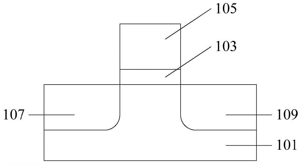
[0029] refer to figure 1 , is a schematic cross-sectional structure diagram of a P-type tunneling field effect transistor in the prior art, including: a semiconductor substrate 101; a gate structure located on the semiconductor substrate 101, the gate structure comprising a high The k dielectric layer 103 and the metal gate 105 located on the high-k dielectric layer 103; the source 107 is located in the semiconductor substrate 101 on one side of the gate structure; the drain 109 is located between the gate structure and In the semiconductor substrate 101 on the side opposite to the source. Wherein, the conductivity type of the semiconductor substrate 101 and the drain 109 is P type, and the conductivity type of the source 107 is N type. Since the operating current of the tunneling field effect transistor is proportional to the tunneling area of ​​the PN junction in the tunneling field effect transistor, and figure 1 The PN junction tunneling area of ​​the medium tunneling fi...


PUM


Abstract

A tunneling field effect transistor and a forming method thereof are provided. The tunneling field effect transistor comprises a semiconductor substrate including a fin, a gate structure across the middle of the fin, a source across one end of the fin, and a drain disposed at the other end of the fin, wherein the conductivity type of the drain is a first conductivity type, and the conductivity type of the source is a second conductivity type different from the first conductivity type. The PN junction tunneling area of the tunneling field effect transistor provided by the invention is large, the working current of the tunneling field effect transistor is high, and the response speed of a device including the tunneling field effect transistor is increased.

Description

technical field [0001] The invention relates to the technical field of semiconductor manufacturing, in particular to a tunnel field effect transistor and a forming method thereof. Background technique [0002] Metal-Oxide-Semiconductor (MOS) technology has been widely used. For example, Complementary Metal Oxide Semiconductor (CMOS) transistors have become core components in semiconductor integrated circuits. In order to continuously improve the performance and packaging density of integrated circuits, and to reduce the cost of integrated circuits, the feature size of CMOS transistors is continuously reduced. [0003] However, as the dimensions of CMOS transistors continue to shrink, the overall power consumption of CMOS transistors continues to increase. The reasons are as follows: 1. The short channel effect becomes more and more obvious (such as the leakage current increases); 2. It is difficult to make the power supply voltage continue to decrease as the size of the CMO...

Claims


Application Information

Patent Timeline
Patent Type & Authority Applications(China)
IPC IPC(8): H01L29/78H01L29/423H01L29/08H01L21/336H01L21/28
CPCH01L29/7391H01L29/78H01L29/0847H01L29/401H01L29/41725H01L29/66477
Inventor 黄新运丁士成
Owner SEMICON MFG INT (SHANGHAI) CORP
Why Eureka
Try Eureka