Crystal edge cleaning device

A technology for cleaning equipment and equipment, applied in cleaning methods and utensils, cleaning methods using liquids, cleaning methods using gas flow, etc., can solve problems such as the impact of product yield improvement, difficult product crystal edge quality, etc. degree, improve product yield, and reduce the effect of possibility

Inactive Publication Date: 2015-03-25
SHANGHAI HUALI MICROELECTRONICS CORP
View PDF9 Cites 10 Cited by
  • Summary
  • Abstract
  • Description
  • Claims
  • Application Information

AI Technical Summary

Problems solved by technology

In production, it is found that it is difficult to effectively control the quality of the product's crystal edge with existing means, and the product's crystal edge often becomes the source of defects, which has a great impact on the improvement of product yield. Therefore, it is urgent to provide a new method to make the chip Effective bezel system processing is carried out throughout the production process to maximize the quality of chip bezels

Method used


Image

  • Crystal edge cleaning device

Examples


Embodiment Construction

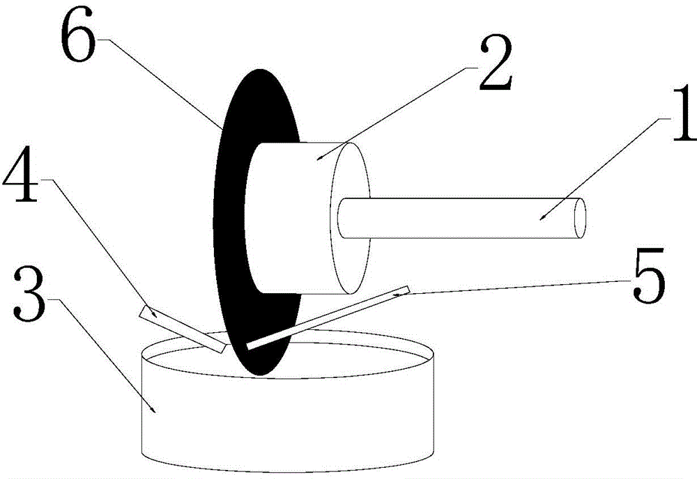
[0017] In view of the current actual production, the crystal edge of the product often becomes the source of defects, so a new equipment is proposed to effectively process the crystal edge in the whole process of production.

[0018] The invention relates to a crystal edge cleaning equipment, comprising a rotating shaft, a wafer clamping device, a cleaning tank and a gas nozzle, the rotating shaft is arranged horizontally, and a driving motor is connected to the rotating shaft, and the rotating shaft is connected to the wafer clamping device Hinged, the first gas nozzle and the second gas nozzle are respectively set on both sides of the wafer clamping device. When cleaning the wafer, the injection point of the first gas nozzle is located at the front edge of the wafer, and the injection point of the second gas nozzle is located at the edge of the wafer. on the opposite edge.

[0019] The specific embodiments of the present invention will be further described below in conjuncti...


PUM


Abstract

The invention relates to the field of semiconductor yield improvement, in particular to a crystal edge cleaning device. According to the crystal edge cleaning device, the front face and the back face of the crystal edge of a wafer can be processed at the same time, residual film structures and various impurities on the crystal edge can be effectively removed, meanwhile, the crystalline degree of the crystal edge can be improved, then, the probability that the crystal edge is the defect source is reduced, and great help is provided for improving the product yield.

Description

technical field [0001] The invention relates to the field of semiconductor yield improvement, in particular to crystal edge cleaning equipment. Background technique [0002] The manufacturing of the semiconductor industry is changing with each passing day, and the line width of products is constantly decreasing. With the reduction of line width, defects will cause greater damage to product yield, and improving various factors that cause defects has become an important means to improve semiconductor yield. During production, many defects are found to be related to the quality of chip bezels. Good bezel quality can effectively reduce the source of defects, thereby providing a good guarantee for improving chip quality. [0003] In actual production, the exposure machine can be used to control the distance of each layer of graphics from the edge of the chip to the chip, and to remove excess substances. It can also be used to etch the crystal edge in the etching chamber. In pro...

Claims


Application Information

Patent Timeline
Patent Type & Authority Applications(China)
IPC IPC(8): B08B3/04B08B5/02H01L21/67
CPCB08B3/04B08B5/02B08B13/00B08B2203/00B08B2205/00H01L21/67
Inventor 何理许向辉叶林
Owner SHANGHAI HUALI MICROELECTRONICS CORP
Why Eureka
Try Eureka