Method for laser pulse sputtering deposition preparation of polycrystalline silicon thin film

A technology of polysilicon thin film and sputtering deposition, which is applied in the growth of polycrystalline materials, chemical instruments and methods, and crystal growth, can solve the problems of unfavorable batch production, limited application of devices, and high requirements for substrates, and achieve a good degree of crystallization , good combination and good repeatability

Inactive Publication Date: 2015-07-22
DALIAN UNIV
View PDF8 Cites 4 Cited by
  • Summary
  • Abstract
  • Description
  • Claims
  • Application Information

AI Technical Summary

Problems solved by technology

[0004] In order to solve the problems of high deposition temperature, high substrate requirements, limited application of devices due to micro-twin crystal defects, and unfavorable mass production in the preparation of polysilicon thin films in the prior art, the present invention provides a method of using PLD technology on copper substrates and Method for preparing polysilicon film on quartz glass substrate

Method used


Image

  • Method for laser pulse sputtering deposition preparation of polycrystalline silicon thin film
  • Method for laser pulse sputtering deposition preparation of polycrystalline silicon thin film
  • Method for laser pulse sputtering deposition preparation of polycrystalline silicon thin film

Examples


Embodiment 1

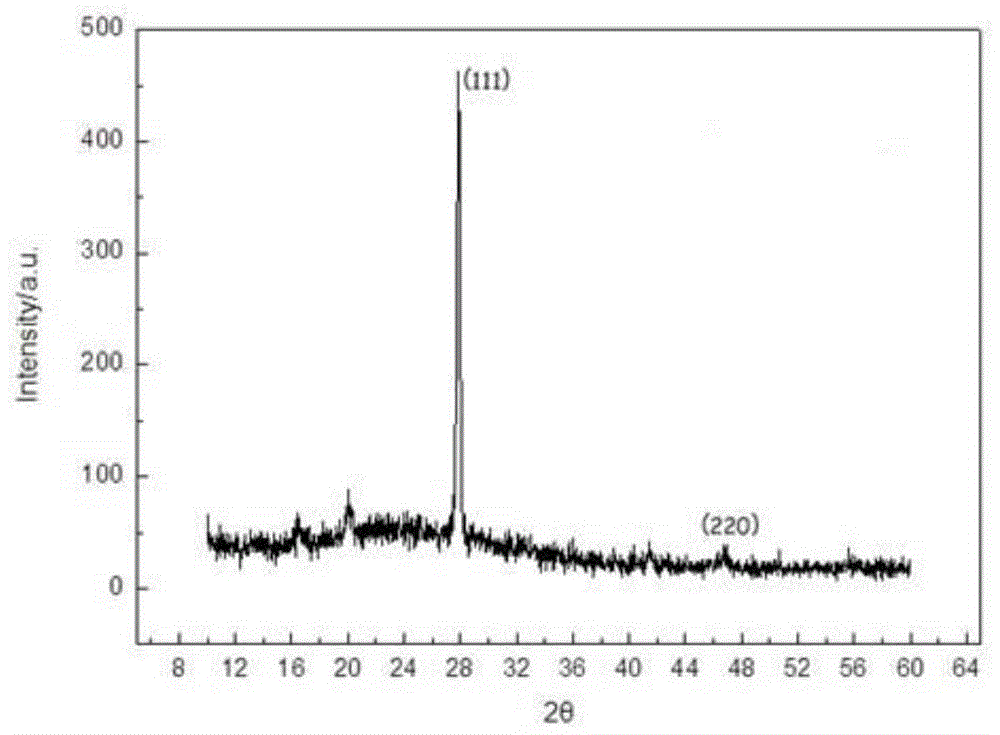
[0026] The coating material is selected as a 99.99% silicon target, and the substrate is a 20*35*3mm copper sheet. First, the copper substrate is pre-treated: the copper substrate is mechanically polished, cleaned with deionized water, firstly ultrasonicated in acetone for 10 minutes, then cleaned with absolute ethanol for 10 minutes and then dried; then the silicon target and the copper substrate are placed Into the PLD-450 vacuum system, vacuum to 1.0×10 -4 Pa, the temperature of the copper substrate is 600°C, the distance between the copper substrate and the silicon target is 4cm, and then the TOL-25B excimer laser is used as the laser source to emit laser light at a frequency of 4HZ, sputtering for 3 hours, and finally after Annealed at 800°C to prepare a polysilicon film.

[0027] Such as figure 1 Shown is that the polysilicon thin film prepared in Example 1 carries out XRD test at room temperature, and the characteristic diffraction peak of crystalline silicon appears ...

Embodiment 2

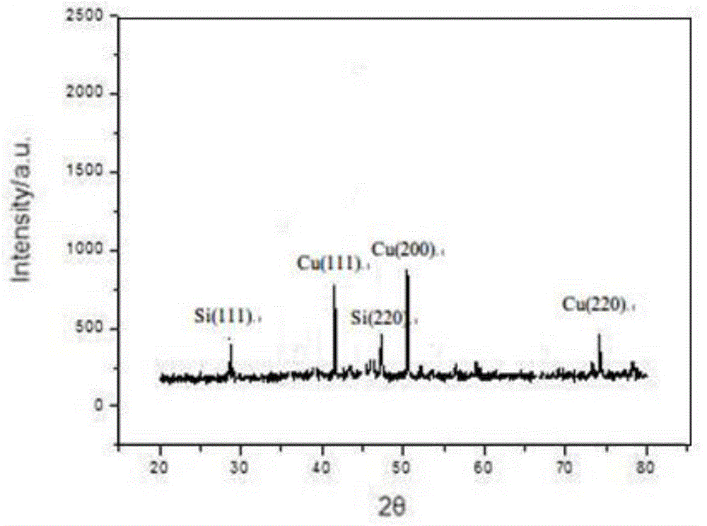
[0031] The coating material is selected as 99.99% silicon target material, and the substrate is 30*30*3mm quartz glass. First, the quartz glass substrate is pre-treated: the quartz glass substrate is cleaned with deionized water, ultrasonicated in acetone for 10 minutes, cleaned with absolute ethanol for 10 minutes, and then dried; the silicon target material of the coating material and the quartz glass substrate are placed in a PLD-450 vacuum system, evacuate to 1.0 x 10 -4 Pa, the temperature of the quartz glass substrate is 600°C, the distance between the quartz glass substrate and the silicon target is 4cm; then the TOL-25B excimer laser is used as the laser source to emit laser light, the frequency is 4HZ, and the sputtering is 3h; finally after 800 ℃ annealing for 3h to prepare a polysilicon film.

[0032] The polysilicon thin film prepared in embodiment 2 is carried out XRD test at room temperature, by figure 2 It can be seen that the characteristic diffraction peaks...

Embodiment 3

[0036] The coating material is selected as a 99.99% silicon target, and the substrate is a 20*35*3mm copper sheet. First, pre-treat the copper substrate: mechanically polish the copper substrate, wash it with deionized water, ultrasonicate it in acetone for 10 minutes, clean it with absolute ethanol for 10 minutes, and then dry it; then put the silicon target and copper substrate into the PLD-450 vacuum system, evacuate to 1.0 x 10 -4Pa, the temperature of the copper substrate is 500°C, the distance between the copper substrate and the silicon target is 3cm, and then the TOL-25B excimer laser is used as the laser source to emit laser light at a frequency of 4HZ, sputtering for 3 hours, and finally after Annealed at 600°C to prepare a polysilicon film.


PUM

PropertyMeasurementUnit
sizeaaaaaaaaaa

Abstract

The invention relates to a method for laser pulse sputtering deposition preparation of a polycrystalline silicon thin film, wherein the method includes the following steps: pre-treating a base plate; putting a film plating material silicon target and the base plate into a vacuum system, vacuumizing to 1.0*10<-4> Pa, wherein the base plate temperature is 500-700 DEG C, and the distance between the base plate and the silicon target is 3-8 cm; then taking an excimer laser as a laser source, emitting laser, and with the frequency of 2-5 HZ, sputtering for 2-4 h; and finally annealing for 2-4 h at the temperature of 600-1000 DEG C, and thus obtaining the polycrystalline silicon thin film, wherein the base plate is a copper sheet or quartz glass. The prepared polycrystalline silicon thin film has fine grains and uniform size distribution, has quite good smoothness and compactness, has a better crystallization degree, moreover, has hardly any impurity atoms, can produce fine grains on various base plates, and is simple in process, good in repeatability, low in cost and suitable for industrialized production.

Description

technical field [0001] The invention relates to a method for preparing a polysilicon film, in particular to a method for preparing a polysilicon film by laser pulse sputtering deposition. Background technique [0002] Polycrystalline silicon thin film not only has the electrical characteristics of crystalline silicon, but also has high ion mobility and light absorption rate, so it has a wide range of applications in modern technology, such as: solar cells, piezoresistive sensors, LCD TVs and other fields. At present, the methods for preparing polysilicon thin films mainly include: liquid phase epitaxy (LPE), chemical vapor deposition (CVD), low pressure chemical vapor deposition (LPCVD), hot wire chemical vapor deposition (HWCVD), and solid phase crystallization (SPC). ), excimer laser annealing (ELA) and metal induction (MIC). However, liquid phase epitaxy (LPE) and chemical vapor deposition (CVD) require a high deposition temperature and have high requirements on the subs...

Claims


Application Information

Patent Timeline
Patent Type & Authority Applications(China)
IPC IPC(8): C30B28/12C30B29/06
Inventor 王宙骆旭梁董桂馥付传起雍帆张庆乐
Owner DALIAN UNIV
Why Eureka
Try Eureka