Low-temperature polycrystalline silicon thin film transistor array substrate and manufacturing method thereof

A thin-film transistor and low-temperature polysilicon technology, applied in the field of transistor manufacturing, can solve the problems of difficult control, complex process, and high density of defect states at the grain boundary, and achieve the effects of reducing the crystallization cooling rate, prolonging the growth time, and improving the thermal insulation effect.

Active Publication Date: 2017-02-01
KUNSHAN GO VISIONOX OPTO ELECTRONICS CO LTD
View PDF4 Cites 4 Cited by
  • Summary
  • Abstract
  • Description
  • Claims
  • Application Information

AI Technical Summary

Problems solved by technology

However, to form crystallized polysilicon by the above method, it is first necessary to form a concave arc surface on the oxide layer 1, and then perform laser crystallization. After the crystallization is completed, the oxide layer is removed. The process is more complicated and difficult to control; The laser light at the curved surface is refracted, so the crystallization effect of the polysilicon under the concave curved surface area will be poor, the overall crystallization uniformity of the polysilicon will be deteriorated, and the defect state density at the grain boundary will be higher, which will seriously affect the thin film transistor. electrical characteristics

Method used


Image

  • Low-temperature polycrystalline silicon thin film transistor array substrate and manufacturing method thereof
  • Low-temperature polycrystalline silicon thin film transistor array substrate and manufacturing method thereof
  • Low-temperature polycrystalline silicon thin film transistor array substrate and manufacturing method thereof

Examples


Embodiment Construction

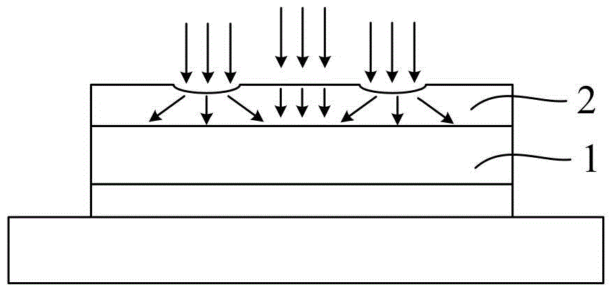
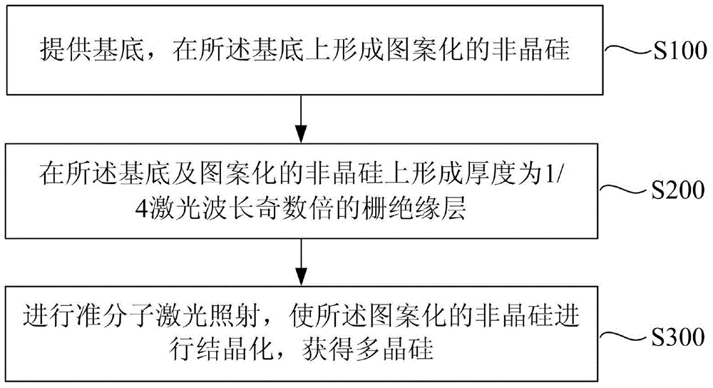
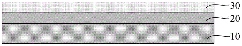
[0027] The low-temperature polysilicon thin film transistor array substrate and its manufacturing method of the present invention will be described in more detail below in conjunction with schematic diagrams, wherein a preferred embodiment of the present invention is shown, it should be understood that those skilled in the art can modify the present invention described here, and still The advantageous effects of the present invention are realized. Therefore, the following description should be understood as the broad knowledge of those skilled in the art, but not as a limitation of the present invention.

[0028] In the interest of clarity, not all features of an actual implementation are described. In the following description, well-known functions and constructions are not described in detail since they would obscure the invention with unnecessary detail. It should be appreciated that in the development of any actual embodiment, numerous implementation details must be worke...


PUM

PropertyMeasurementUnit
wavelengthaaaaaaaaaa
thicknessaaaaaaaaaa
thicknessaaaaaaaaaa

Abstract

The invention provides a low-temperature polycrystalline silicon thin film transistor array substrate and a manufacturing method thereof. A gate insulation layer whose thickness is the odd number times a 1 / 4 laser wavelength on a patterned amorphous silicon to serve as an insulation layer. As the thickness of the gate insulation layer is the odd number times the 1 / 4 laser wavelength, the laser can pass through the gate insulation layer to the maximum degree to reach the patterned amorphous silicon, good crystallization processing is carried out on the patterned amorphous silicon, and large crystal grains are acquired. As the surface of the gate insulation layer is uniform, the passing laser thus uniformly irradiates on the patterned amorphous silicon, and the polycrystalline silicon with uniform crystal grains is thus formed.

Description

technical field [0001] The invention relates to the field of transistor manufacturing, in particular to a low-temperature polysilicon thin film transistor array substrate and a manufacturing method thereof. Background technique [0002] At present, TFT (Thin Film Transistor, thin-film transistor) used in AMOLED (Active-matrix organic light emitting diode, active-matrix organic light-emitting diode or active-matrix organic light-emitting diode) mostly uses low-temperature polysilicon as the active layer. The method of manufacturing TFT on AMOLED is to first form a buffer layer on a glass substrate, then deposit an amorphous silicon film on the buffer layer, and then perform a crystallization process of excimer laser annealing on the amorphous silicon film. Before the crystallization process, it needs The amorphous silicon film is cleaned, and an extremely thin oxide film is formed on the amorphous silicon film to form an insulating layer to reduce the cooling rate of crystall...

Claims


Application Information

Patent Timeline
Patent Type & Authority Applications(China)
IPC IPC(8): H01L21/77H01L27/12
CPCH01L27/1214H01L27/1274H01L27/1281H01L27/1285
Inventor 赵雁飞李建文魏博
Owner KUNSHAN GO VISIONOX OPTO ELECTRONICS CO LTD
Why Eureka
Try Eureka