Cutting method of crystalline silicon ingot

A cutting method and technology of crystalline silicon, applied in fine working devices, manufacturing tools, stone processing equipment, etc., can solve problems such as long production cycle

Active Publication Date: 2015-03-25
JIANGSU XIEXIN SILICON MATERIAL TECH DEV
View PDF5 Cites 5 Cited by
  • Summary
  • Abstract
  • Description
  • Claims
  • Application Information

AI Technical Summary

Problems solved by technology

Then the whole polysilicon ingot is cut, the process is as follows figure 1 As shown: First, the whole silicon ingot is vertically squared into 5×5 or 6×6 small square ingots, and then the head and tail material of the small square ingots are cut off, and then the cut small square ingots are sliced ​​to obtain The grain orientation of the polycrystalline silicon wafer is perpendicular to the growth direction of the columnar grains of the silicon ingot. There are many grain boundaries in the silicon wafer, and the three-step process of square extraction, truncation, and slicing is required, and the production cycle is longer.

Method used


Image

  • Cutting method of crystalline silicon ingot
  • Cutting method of crystalline silicon ingot
  • Cutting method of crystalline silicon ingot

Examples


Embodiment Construction

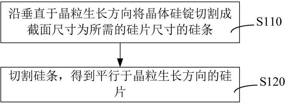
[0014] figure 2 A flow chart illustrating a method for cutting a crystalline silicon ingot according to the present invention. Combine below image 3 ,A detailed description figure 2 Implementation of the method shown.

[0015] The flow chart of the method for cutting a crystalline silicon ingot of the present invention includes the following steps.

[0016] Step S110 , cutting the crystalline silicon ingot into silicon strips with a cross-sectional size equal to the required silicon chip size along the direction perpendicular to the grain growth direction.

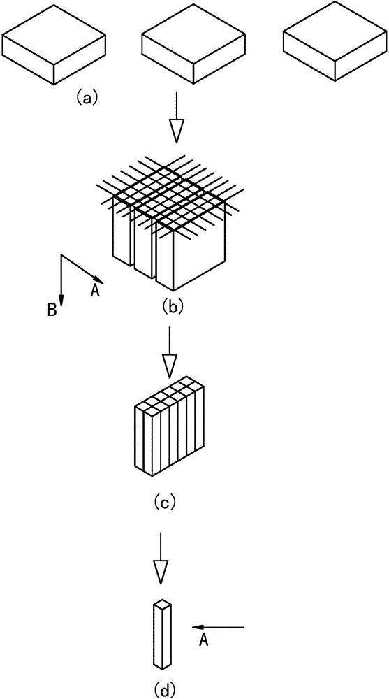
[0017] For details, please refer to image 3 , including the following steps:

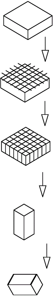
[0018] (a) First erect the crystalline silicon ingot. After being erected, one side of the crystalline silicon ingot rests on the square tray, and the opposite side is used for wiring.

[0019] (b) Wiring is carried out on the side surface of the crystalline silicon ingot according to the required silicon wafer size. In the tradition...


PUM

PropertyMeasurementUnit
Sizeaaaaaaaaaa

Abstract

The invention relates to a cutting method of a crystalline silicon ingot. The cutting method comprises the steps that the crystalline silicon ingot is cut in the direction perpendicular to the grain growth direction into silicon bars with the section size equal to the size of needed silicon wafers; the silicon bars are cut to obtain the silicon wafers with the grain direction parallel with the grain growth direction. According to the cutting method, the crystalline silicon wafers with the grain direction parallel with the grain growth direction are directly obtained through one-time radication and one-time wafer cutting, the cutting-off process is omitted, the production cycle is shortened, production efficiency is improved, the large-grain polycrystalline silicon wafers with the grain direction parallel with the grain growth direction can be obtained, grain boundaries are reduced, and the quality of the silicon wafers is improved.

Description

technical field [0001] The invention relates to the technical field of polycrystalline silicon slicing, in particular to a method for cutting crystalline silicon ingots. Background technique [0002] Polysilicon is currently one of the most important substrate materials in the solar cell industry. According to different growth methods, the temperature gradient of the solid-liquid interface is controlled during the solidification process to form a unidirectional heat flow, and the controllable directional solidification will form a physical and mechanical property Anisotropic polycrystalline columnar crystals, most of the current polycrystalline silicon ingots are produced by this directional solidification method, and the orientation of the polycrystalline grains obtained by casting the ingot is perpendicular to the bottom surface of the crucible. Then the whole polysilicon ingot is cut, the process is as follows figure 1 As shown: First, the whole silicon ingot is vertical...

Claims


Application Information

Patent Timeline
IPC IPC(8): B28D5/00
CPCB28D5/0005
Inventor 周声浪游达胡亚兰王双丽田义良
Owner JIANGSU XIEXIN SILICON MATERIAL TECH DEV
Why Eureka
Try Eureka