

Novel tin oxide semiconductor and preparation method and application thereof
A tin dioxide and semiconductor technology, which is applied in the field of novel tin dioxide semiconductor photocatalyst and its preparation, can solve the problems of less research on visible photosynthesis, limited application and the like
Active Publication Date: 2015-03-25
GUIZHOU UNIV
View PDF1 Cites 14 Cited by
- Summary
- Abstract
- Description
- Claims
- Application Information
AI Technical Summary
Problems solved by technology
1. SnO 2 It is a wide bandgap semiconductor material (3.6-3.8eV) which limits its application in photocatalytic / photoelectrochemical water splitting
2. There are still relatively few studies on its visible photochemistry, and the relevant theories are not enough
Method used
View moreImage
Smart ImageViewing Examples

Examples
Embodiment 1
Embodiment 2
Embodiment 3
Login to View More PUM
| Property | Measurement | Unit |
|---|---|---|
| particle size | aaaaa | aaaaa |
| size | aaaaa | aaaaa |
Abstract
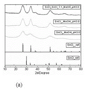
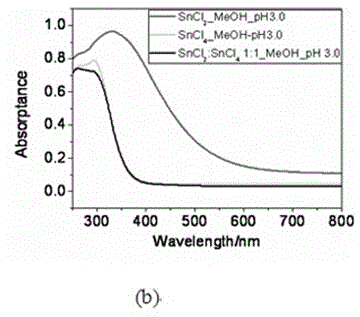
The invention provides a novel tin oxide semiconductor photocatalyst. A bivalent chloride of tin SnCl2.2H2O or a bivalent bromide of tin SnBr2.2H2O is dissolved in methanol or ethanol, and a hydrothermal reaction is carried out in a hydrothermal reaction kettle at 150 DEG C to obtain a SnO2 nano semiconductor material with visible light response, wherein the average grain size is 2.5nm, the absorption edge of single-phase SnO2 powder reaches 570nm and is corresponding to a bandgap of 2.17eV, higher light anode current is displayed within a visible wavelength range and reaches a mA / cm<2> level, and half reaction activity of producing hydrogen and oxygen is also achieved. The preparation method comprises the following steps: dissolving the bivalent chloride of tin SnCl2.2H2O or the bivalent bromide of tin SnBr2.2H2O in methanol or ethanol to prepare an alcoholic solution with concentration of 20mmol / L, carrying out the hydrothermal reaction in the hydrothermal reaction kettle at 150 DEG C for at least 24 hours, standing, filtering, and drying filtrate solid at 50-80 DEG C to obtain the novel tin oxide semiconductor photocatalyst. The application comprises: preparing the product into a photoelectrode. Under visible light response, the photoelectrode has higher photoelectrochemical water splitting activity, so that the photoelectrode is used for photocatalytic water splitting or is used as a visible-light-induced photocatalyst.
Description
technical field The invention belongs to the development field of new functional materials, in particular to a novel tin dioxide semiconductor photocatalyst and its preparation method and application. Background technique Photoelectrochemical / photocatalytic water splitting is widely recognized for converting solar energy into chemical energy H 2 ideal way. The generally accepted principle of solar photocatalysis / photoelectrochemical water splitting is that when a semiconductor photocatalyst is excited by photons with energy greater than its band gap, electrons jump from the top of the valence band to the bottom of the conduction band, thereby generating photogenerated holes in the valence band. When the conduction band bottom of the semiconductor photocatalyst is higher / negative than H + / H 2 The reduction potential of the valence band is lower / positive than that of H 2 O / O 2 When the oxidation potential is high, photogenerated electrons and holes have the ability to re...
Claims
Login to View More Application Information
Patent Timeline
 Patent Type & AuthorityApplications(China)
IPC IPC(8): C01G19/02B01J23/14
CPCB01J23/14C01G19/02
Inventor田蒙奎
OwnerGUIZHOU UNIV