Wafer testing system and method

A wafer testing and wafer technology, applied in the electronic field, can solve the problems of inflexible testing, high cost, long cycle, etc., and achieve the effect of shortening the testing cycle, reducing the testing cost and improving the testing efficiency

Active Publication Date: 2015-03-25
NAT CENT FOR ADVANCED PACKAGING CO LTD
View PDF14 Cites 9 Cited by
  • Summary
  • Abstract
  • Description
  • Claims
  • Application Information

AI Technical Summary

Problems solved by technology

However, since the thinned wafer is only a few hundred microns thick, it is very fragile and fragile, and cannot be fixedly placed on the current flying probe tester.
At the same time, the sample to be tested on the flying probe testing machine is determined based on the copper frame on the rectangular substrate as the approximate reference position, which cannot be aligned with the reference position of the circular wafer to be tested.
In the existing technology, automatic probe stations need to be purchased for wafer testing, and different probe cards need to be customized for different wafer layouts. The testing is inflexible, costly, and has a long cycle, which is not conducive to the industrialization process of SIP technology.

Method used


Image

  • Wafer testing system and method
  • Wafer testing system and method
  • Wafer testing system and method

Examples


Embodiment Construction

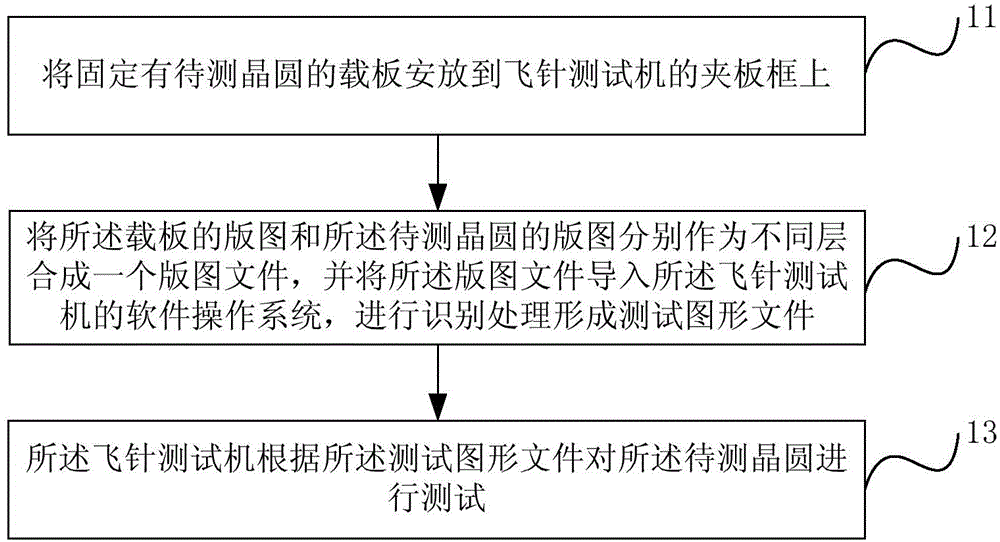
[0034] The present invention will be further described in detail below in conjunction with the accompanying drawings and embodiments. It should be understood that the specific embodiments described herein are only used to explain the present invention, but not to limit the present invention. In addition, it should be noted that, for the convenience of description, the drawings only show some but not all of the contents related to the present invention.

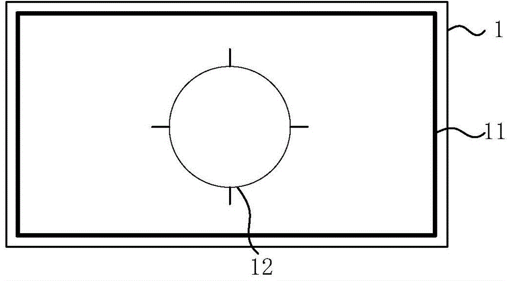
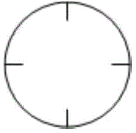
[0035] figure 1 is a schematic diagram of a carrier board in a wafer testing system provided by an embodiment of the present invention, figure 2 It is a schematic diagram of a wafer to be tested in a wafer testing system provided by an embodiment of the present invention. The following is combined with figure 1 and figure 2 to describe the embodiments of the present invention.

[0036] The wafer testing system includes a flying probe tester and a carrier board, the flying probe tester is used to test the wafer to be test...


PUM


Abstract

The invention discloses a wafer testing system and method. The system comprises a flying-probe tester and a carrier plate, the flying-probe tester is used for testing a wafer to be tested, the carrier plate is used for bearing the wafer to be tested on the flying-probe tester and providing an alignment mark corresponding to a clamping plate frame of the flying-probe tester and the domain of the carrier plate, the domain of the carrier plate and the domain of the wafer to be tested are matched to form a domain file to be tested, and after the domain file to be tested is led into a software operation system of the flying-probe tester, a testing figure file is formed. According to the wafer testing system and method, various pinboard wafers or wafers of passive integrated devices can be automatically tested through the flying-probe tester, an automatic probe table does not need to be bought for testing the wafer with different domains, corresponding expansive probe cards do not need to be customized according to the wafers to be tested with the different domains, the flexibility is improved, the cost is lowered, the period is shortened, and the industrialization process of the wafer pinboarrds such as TSV and TGV and an IPD technology is promoted.

Description

technical field [0001] The present invention relates to the field of electronic technology, in particular to a wafer testing system and a wafer testing method. Background technique [0002] With the rapid development of electronic products, the microelectronic packaging technology is developing towards the trend of multi-function, miniaturization, portability, high speed, low power consumption and high reliability. System-in-a-Package (SIP) can effectively reduce the chip area, power consumption and heat dissipation. The technology of making interposers and LCR devices on wafers, such as Through Silicon Via (TSV) Technology, through glass via wafer (TGV) technology and integrated passive device (Integrated Passive Device, IPD) technology are important technologies for SIP packaging, so they have received more and more attention. [0003] At present, there is no automatic test equipment specifically for wafer-type adapter boards, which has become one of the bottlenecks in re...

Claims


Application Information

Patent Timeline
Patent Type & Authority Applications(China)
IPC IPC(8): G01R31/26
Inventor 杜天敏
Owner NAT CENT FOR ADVANCED PACKAGING CO LTD
Why Eureka
Try Eureka