Schottky diode and manufacturing method thereof

A technology of Schottky diodes and anodes, applied in the direction of diodes, semiconductor/solid-state device manufacturing, electrical components, etc., can solve problems such as large leakage

Active Publication Date: 2015-03-25
GPOWER SEMICON
View PDF7 Cites 12 Cited by
  • Summary
  • Abstract
  • Description
  • Claims
  • Application Information

AI Technical Summary

Problems solved by technology

The Schottky diode can solve the problem of large leakage current of the metal / two-dimensional electron gas Schottky junction under the anode reverse bias voltage in the GaN heterostructure in the prior art

Method used


Image

  • Schottky diode and manufacturing method thereof
  • Schottky diode and manufacturing method thereof
  • Schottky diode and manufacturing method thereof

Examples


Embodiment 1

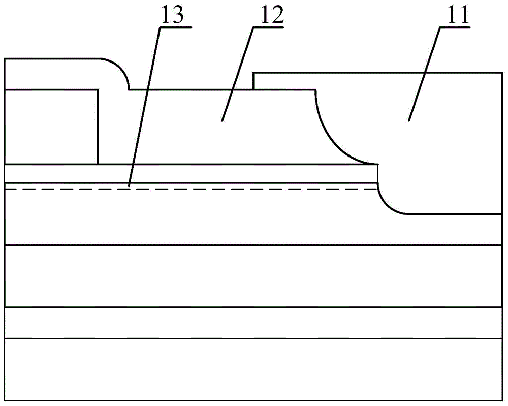
[0060] Figure 4 A schematic cross-sectional view of the Schottky diode provided in Embodiment 1 of the present invention is given. Such as Figure 4 shown, the Schottky diode consists of:

[0061] A substrate 1, wherein the material of the substrate 1 can be gallium nitride, silicon, sapphire, silicon nitride, aluminum nitride, SOI or other substrate materials that can epitaxially grow III-V group nitrides.

[0062] A nucleation layer 2, a buffer layer 3, a first semiconductor layer 4 and a second semiconductor layer 6 grown sequentially on a substrate 1, wherein the band gap of the first semiconductor layer 4 is smaller than the band gap of the second semiconductor layer 6 , the material of the nucleation layer 2 can be aluminum nitride or gallium nitride, the material of the buffer layer 3 can be a graded layer of aluminum gallium nitride or a superlattice material, and the material of the first semiconductor layer 4 can be gallium nitride, The material of the second sem...

Embodiment 2

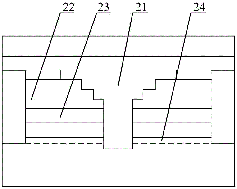
[0082] Figure 8 A schematic cross-sectional view of the Schottky diode provided in Embodiment 2 of the present invention is given.

[0083] Such as Figure 8 As shown, different from the first embodiment, the anode trench of the Schottky diode provided by the second embodiment extends into the second semiconductor layer 6 , but does not exceed the second semiconductor layer 6 . After the second semiconductor layer is etched and thinned, the concentration of the two-dimensional electron gas under it will decrease, resulting in an increase in the on-resistance. If the etching depth is too deep, the two-dimensional electron gas will be depleted, and the diode’s The forward voltage will increase. Therefore, the etching depth of the field plate trench needs to be controlled within a reasonable range. Generally speaking, the distance between the bottom of the trench and the two-dimensional electron gas channel needs to be greater than 5 nm to ensure a normal conduction of two-dim...

Embodiment 3

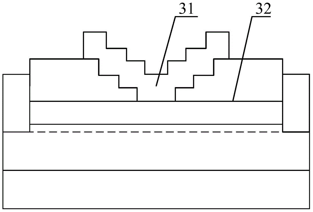
[0086] Figure 9 A schematic cross-sectional view of the Schottky diode provided by Embodiment 3 of the present invention is given.

[0087] Such as Figure 9 As shown, different from Embodiment 1, the Schottky diode provided in Embodiment 3 also includes:

[0088] The field plate trench dielectric layer 10 is located on the passivation dielectric layer 8 and on the field plate trench.

[0089] In this embodiment, the material of the field plate trench dielectric layer 10 may be any one or a combination of at least two of silicon nitride, silicon dioxide, silicon oxynitride or aluminum oxide.

[0090] Compared with the Schottky diode provided in the first embodiment of the present invention, in the anode structure of the Schottky diode provided in the third embodiment of the present invention, a field plate trench dielectric layer is added between the field plate trench and the anode, which can further Reduces the leakage current flowing through the Schottky junction in the...


PUM


Abstract

The invention discloses a Schottky diode and a manufacturing method thereof. The Schottky diode comprises a substrate, a first semiconductor layer located on the substrate, a second semiconductor layer located on the first semiconductor layer, two-dimensional electron gas formed at the interface of the first semiconductor layer and the second semiconductor layer, a cathode located on the second semiconductor layer, a first passivation dielectric layer located on the second semiconductor layer, an anode groove located between the first passivation dielectric layer and the second semiconductor layer, a field plate groove located in the part, between the anode groove and the cathode, of the first passivation layer, and an anode covering the anode groove, the field plate groove and the part, between the anode groove and the field plate groove, of the first passivation dielectric layer. The Schottky diode has the advantages of being low in forward conduction voltage and reverse electric leakage and resistant to high voltage.

Description

technical field [0001] The invention relates to the field of semiconductors, in particular to a Schottky diode and a manufacturing method thereof. Background technique [0002] In the application field of high-voltage switches, it is hoped that the diode has the characteristics of small reverse leakage, large reverse withstand voltage and small forward conduction voltage drop. Power electronic devices based on wide-bandgap semiconductor materials, especially gallium nitride materials, have superior properties. Therefore, Gallium Nitride Schottky diodes have gradually become a research hotspot in recent years. The technology of homoepitaxial GaN on GaN substrate is still in the stage of small size and high cost. Although high-quality epitaxial materials and ideal device performance can be obtained, it has not been widely adopted based on cost considerations. use. At present, gallium nitride materials are mainly obtained by epitaxial growth on heterogeneous materials, and t...

Claims


Application Information

Patent Timeline
Patent Type & Authority Applications(China)
IPC IPC(8): H01L29/872H01L29/06H01L21/329
CPCH01L29/872H01L29/2003H01L29/205H01L29/402H01L29/404H01L29/407H01L29/417H01L29/66212H01L29/66219H01L29/778H01L29/0684H01L29/66143
Inventor 陈洪维
Owner GPOWER SEMICON
Why Eureka
Try Eureka