SOI power device with medium layer fixed charges
A fixed charge, power device technology, applied in electrical components, semiconductor devices, circuits, etc.
- Summary
- Abstract
- Description
- Claims
- Application Information
AI Technical Summary
Problems solved by technology
Method used
Image

Examples
Embodiment Construction
[0022] The present invention will be further described in detail through specific embodiments and related applications below.
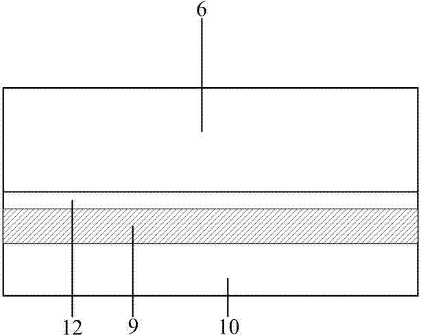
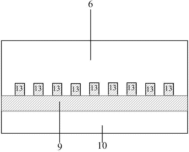
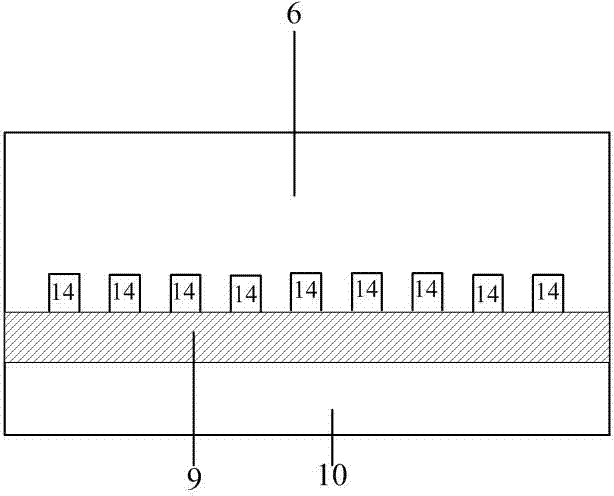
[0023] An SOI power device with a fixed charge in a dielectric layer, comprising a substrate layer 10, an active layer 6, and an insulating dielectric buried layer 9 between the substrate layer and the active layer, where the insulating dielectric buried layer 9 is in contact with the active layer 6 A high-concentration fixed-charge region 11 is set in the side area of the surface, and the area of the high-concentration fixed-charge region 11 accounts for 50%-75% of the surface area of the insulating dielectric buried layer in contact with the active layer. The high-concentration fixed-charge region 11 charges The concentration is 1×10 17 ~1×10 18 / cm 2 .
[0024] The charges injected into the high-concentration fixed charge region can be positive ions of potassium, sodium, boron or silicon. After testing, the devices made by injecting the ab...
PUM
 Abstract
Description
Claims
Application Information
 - R&D
- Intellectual Property
- Life Sciences
- Materials
- Tech Scout
- Unparalleled Data Quality
- Higher Quality Content
- 60% Fewer Hallucinations
Browse by: Latest US Patents, China's latest patents, Technical Efficacy Thesaurus, Application Domain, Technology Topic, Popular Technical Reports.
© 2025 PatSnap. All rights reserved.Legal|Privacy policy|Modern Slavery Act Transparency Statement|Sitemap|About US| Contact US: help@patsnap.com