Method of forming semiconductor device

A semiconductor and device technology, which is applied in the field of semiconductor device formation, can solve the problems of the semiconductor substrate being easily damaged, affecting the electrical performance of the semiconductor device, etc., and achieve the effects of improving electrical performance, optimizing electrical performance, and improving reliability.

Active Publication Date: 2017-09-22
SEMICON MFG INT (SHANGHAI) CORP
View PDF4 Cites 0 Cited by
  • Summary
  • Abstract
  • Description
  • Claims
  • Application Information

AI Technical Summary

Problems solved by technology

[0005] However, the semiconductor substrate of the semiconductor device formed in the prior art is easily damaged, which affects the electrical performance of the semiconductor device

Method used


Image

  • Method of forming semiconductor device
  • Method of forming semiconductor device
  • Method of forming semiconductor device

Examples


Embodiment Construction

[0029] As mentioned in the background, the electrical performance of semiconductor devices formed in the prior art is poor.

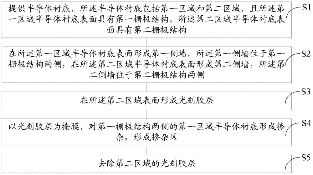
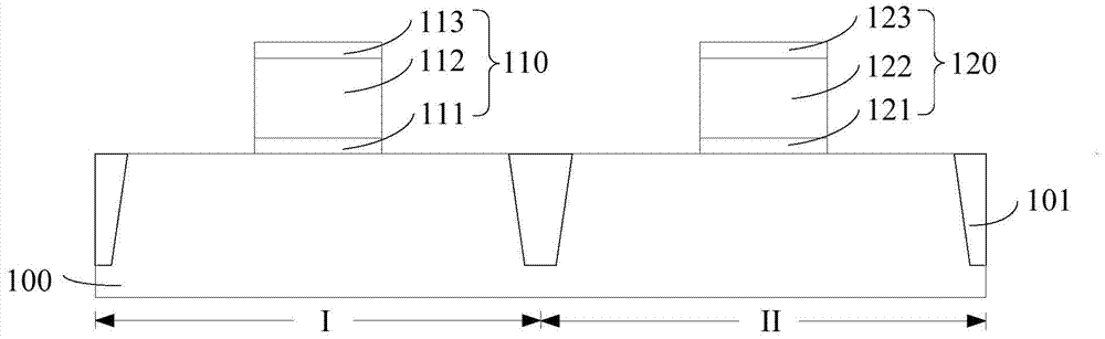
[0030] To this end, research is conducted on the formation method of semiconductor devices. The formation method of semiconductor devices includes the following steps, please refer to figure 1 : Step S1, providing a semiconductor substrate, the semiconductor substrate includes a first region and a second region, and the surface of the semiconductor substrate in the first region has a first gate structure, and the surface of the semiconductor substrate in the second region has The second gate structure; step S2, forming first sidewalls on the surface of the semiconductor substrate in the first region, the first sidewalls are located on both sides of the first gate structure, and on the surface of the semiconductor substrate in the second region Forming second sidewalls, the second sidewalls are located on both sides of the second gate structure; step S3,...


PUM


Abstract

A method for forming a semiconductor device, comprising: providing a semiconductor substrate, the semiconductor substrate includes a first region and a second region, the surface of the semiconductor substrate in the first region has a first gate structure, and the second region The surface of the semiconductor substrate has a second gate structure; forming a sidewall film covering the first gate structure, the second gate structure and the semiconductor substrate; forming an anti-reflection coating covering the sidewall film; The photoresist layer on the surface of the antireflection coating in the first region; using the photoresist layer as a mask, etch and remove the antireflection coating in the second region; using the photoresist layer as a mask, etching back The sidewall film in the second region is etched to form sidewalls on the surface of the semiconductor substrate in the second region, and the sidewalls are located on both sides of the second gate structure. The invention improves the precision of forming the photoresist layer, avoids damage to the semiconductor substrate caused by the forming process, improves the flatness of the semiconductor substrate, and improves the electrical performance of the semiconductor device.

Description

technical field [0001] The invention relates to the field of semiconductor manufacturing, in particular to a method for forming a semiconductor device. Background technique [0002] In the manufacturing process of semiconductor devices, the photolithography method of exposing and developing the photoresist is the main method to realize pattern transfer, which is used to protect the specific area of ​​the treated lower cladding layer from being etched or doped, usually Yes, the treated lower cladding layer is a semiconductor substrate. [0003] With the development of chip technology, the size of the feature pattern of the chip is getting smaller and smaller, and the material of the undercoat layer to be processed is also more and more diverse. Therefore, during the photolithography exposure process, the gap between the photoresist layer and the undercoat layer is due The exposure reflection problem caused by the difference in optical properties has become an important facto...

Claims


Application Information

Patent Timeline
Patent Type & Authority Patents(China)
IPC IPC(8): H01L21/336H01L21/308
Inventor 胡华勇
Owner SEMICON MFG INT (SHANGHAI) CORP
Why Eureka
Try Eureka