
Trench MOSFET (metal-oxide-semiconductor field effect transistor) and Schottky diode integrated structure with shield grids

A Schottky diode, trench gate technology, applied in electrical components, electrical solid devices, circuits, etc., can solve the problems of high process difficulty, leakage current and the depth of forward conduction voltage drop, etc., to achieve simple process and easy process. Control, reduce the effect of area

Active Publication Date: 2015-04-15
SHANGHAI HUAHONG GRACE SEMICON MFG CORP
View PDF3 Cites 8 Cited by
  • Summary
  • Abstract
  • Description
  • Claims
  • Application Information

AI Technical Summary

Problems solved by technology

[0020] The second type of integration structure is generally used in trench gate MOSFETs with small pitch and trench CT. Its advantage is that the Schottky diode is integrated in the contact hole, and no additional area or mask is required; its disadvantage is that the Schottky diode The leakage current and forward voltage drop (VF) of the tertiary diode are easily affected by the depth of the trench CT, and the process is difficult

Method used


Image

  • Trench MOSFET (metal-oxide-semiconductor field effect transistor) and Schottky diode integrated structure with shield grids
  • Trench MOSFET (metal-oxide-semiconductor field effect transistor) and Schottky diode integrated structure with shield grids
  • Trench MOSFET (metal-oxide-semiconductor field effect transistor) and Schottky diode integrated structure with shield grids

Examples


Embodiment Construction

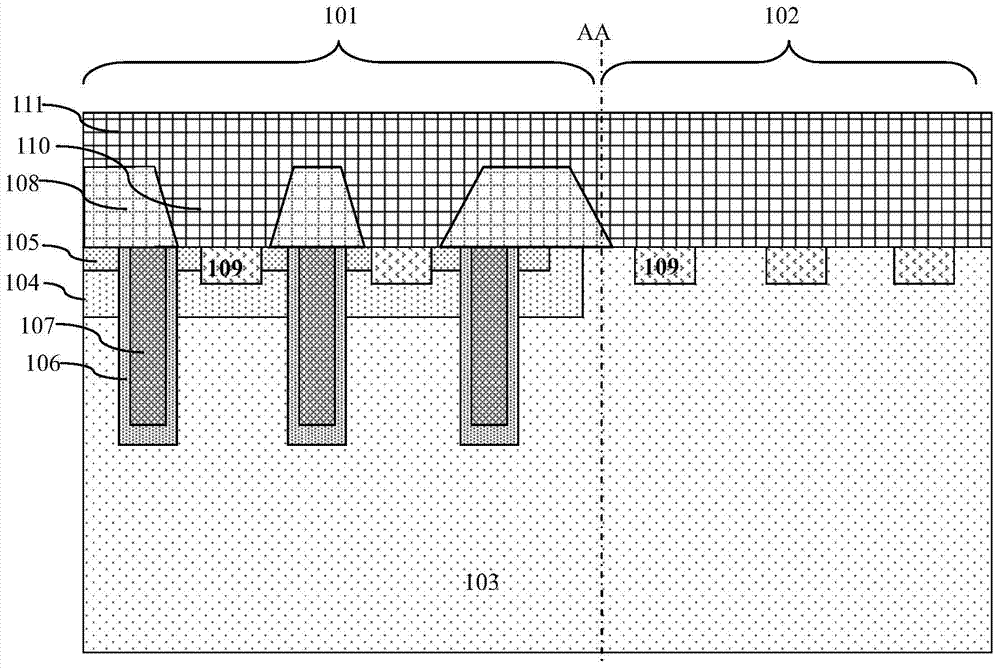
[0046] like Figure 6 Shown is a schematic diagram of an integrated structure of a trench gate MOSFET with a shielded gate and a Schottky diode in an embodiment of the present invention; the integrated structure of the embodiment of the present invention is formed on an N-type heavily doped silicon substrate, and on the silicon substrate The upper part is divided into the formation area 1 of the trench gate MOSFET and the formation area 2 of the Schottky diode. The formation region 1 of the trench gate MOSFET and the formation region 2 of the Schottky diode are separated and adjacent, and the adjacent positions are as follows Figure 6 Shown at the dotted line BB in.

[0047] The cell structure of the trench gate MOSFET in the formation region 1 of the trench gate MOSFET includes:

[0048] N-type doped silicon epitaxial layer 3, the silicon epitaxial layer 3 is formed on the surface of the silicon substrate.

[0049] The P-type well region 4 is formed in the surface region ...


PUM


Abstract

The invention discloses a trench MOSFET (metal-oxide-semiconductor field effect transistor) and Schottky diode integrated structure based on shield grids. The integrated structure is formed on a silicon substrate, and a trench MOSFET forming region and a Schottky diode forming region are separated from and adjacent to each other. A trench MOSFET adopts a double-grid structure with the shield grids, trench structures as same as trench grids are formed in the Schottky diode forming region, Schottky contact is formed on the side faces of trenches by filling front metal layers into the tops of the trenches, and the front metal layers and silicon epitaxial layers outside the trenches also form Schottky contact. The Schottky contact area can be increased greatly by Schottky contact structures on the side faces of and outside the trenches, and the area that the Schottky diode forming region occupies a die can be decreased greatly. Meanwhile, a Schottky diode in the integrated structure is unrelated to source contact holes adopting trench contact holes, and accordingly, performance of the Schottky diode is not affected by the trench contact holes, and technology is simple and easy to control.

Description

technical field [0001] The invention relates to a structure of a semiconductor integrated circuit device, in particular to an integrated structure of a trench gate MOSFET with a shield gate and a schottky diode. Background technique [0002] Integrating Schottky diodes in power MOS transistor devices can improve the cross-frequency characteristics of the devices, such as figure 1 Shown is a schematic diagram of the first integrated structure of an existing trench gate MOSFET with a shielded gate and a Schottky diode; the first integrated structure is formed on an N-type heavily doped silicon substrate, and on the silicon substrate The upper part is divided into a formation area 101 of a trench gate MOSFET and a formation area 102 of a Schottky diode. The formation area 101 of a trench gate MOSFET and the formation area 102 of a Schottky diode are separated and adjacent, and the adjacent positions are as figure 1 Shown at the dotted line AA in. [0003] The unit structure o...

Claims


Application Information

Patent Timeline
IPC IPC(8): H01L27/06H01L29/78H01L29/423H01L29/06H01L29/872
Inventor 陈正嵘陈晨陈菊英
Owner SHANGHAI HUAHONG GRACE SEMICON MFG CORP
Learn More