

Method of variable temperature growth of InAs/GaSb superlattice infrared detector GaSb buffer layer on silicon substrate
An infrared detector, infrared detection technology, applied in semiconductor devices, sustainable manufacturing/processing, electrical components, etc., can solve problems affecting device function, lattice mismatch, etc., to improve the quality of epitaxial layers, reduce defect density, The effect of broad application prospects and technical advantages
- Summary
- Abstract
- Description
- Claims
- Application Information
AI Technical Summary
Problems solved by technology
Method used
Image

Examples
Embodiment 1
[0028] This embodiment provides a method for variable temperature growth of InAs / GaSb superlattice GaSb buffer layer on a silicon substrate, comprising the following steps:
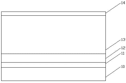
[0029] Step 1: Take a substrate 10, and the material of the substrate 10 is silicon.
[0030] Step 2: growing an AlSb thin layer 11 on the substrate 10 by molecular beam epitaxy. The thickness of the thin layer is 1.5-5nm, and the growth temperature is 500-580°C. The main purpose is to maximize the alleviation of the lattice mismatch between the substrate and the GaSb buffer layer, and form a transition layer, which can greatly reduce the dislocations and defects of the next material growth, and improve the material quality.
[0031] Step 3: growing a GaSb thin layer 12 on the AlSb thin layer 11 at low temperature, the thin layer thickness is 5-10 nm, and the growth temperature is 450-500°C. Since the lattice constants of AlSb and GaSb are similar, the lattice mismatch is small, which is beneficial to r...
Embodiment 2
[0040] This embodiment provides a method for variable temperature growth of InAs / GaSb superlattice GaSb buffer layer on a silicon substrate, comprising the following steps:
[0041] Step 1: Take a silicon substrate 10;
[0042] Step 2: growing an AlSb thin layer 11 on the substrate with a growth temperature of 540° C. and a thickness of 3.6 nm.
[0043] Step 3: On the AlSb thin layer 11, the GaSb thin layer 12 is first grown at low temperature, the growth temperature is 480° C., and the thickness is 8 nm. The purpose of this low-temperature growth GaSb thin layer is to prevent dislocations between the GaSb buffer layer 13 and the AlSb thin layer 11 and the substrate 10 due to lattice mismatch, reduce the dislocation density in the material of the GaSb buffer layer 13, and improve buffering. The crystal quality of the layer material.
[0044] Step 4: Pause for 8 minutes, and adjust the temperature to the next growth temperature.
[0045] Step 5: growing a GaSb buffer layer 1...
Embodiment 3
[0049] This embodiment provides a method for variable temperature growth of InAs / GaSb superlattice GaSb buffer layer on a silicon substrate, comprising the following steps:
[0050] Step 1: Take a silicon substrate 10;
[0051] Step 2: growing an AlSb thin layer 11 on the substrate with a growth temperature of 520° C. and a thickness of 3 nm.
[0052] Step 3: On the AlSb thin layer 11, the GaSb thin layer 12 is first grown at low temperature, the growth temperature is 460° C., and the thickness is 6 nm. The purpose of this low-temperature growth GaSb thin layer is to prevent dislocations between the GaSb buffer layer 13 and the AlSb thin layer 11 and the substrate 10 due to lattice mismatch, reduce the dislocation density in the material of the GaSb buffer layer 13, and improve buffering. The crystal quality of the layer material.
[0053] Step 4: Pause for 10 minutes, and adjust the temperature to the next growth temperature.
[0054] Step 5: growing a GaSb buffer layer 13...
PUM
| Property | Measurement | Unit |
|---|---|---|
| Thickness | aaaaa | aaaaa |
| Thickness | aaaaa | aaaaa |
| Thickness | aaaaa | aaaaa |
Abstract
Description
Claims
Application Information