Preparation method of graphene field-effect transistor biosensor

A technology of field-effect transistors and biosensors, applied in the field of preparation of graphene field-effect transistor biosensors, can solve the problems of affecting the electrical properties of probe-modified graphene, long time, usually more than 2 hours, and expensive preparation equipment. Achieve the effect of retaining superior performance, short copper etching time, and simple preparation method

Active Publication Date: 2015-04-22
HUBEI UNIV OF CHINESE MEDICINE
View PDF6 Cites 23 Cited by
  • Summary
  • Abstract
  • Description
  • Claims
  • Application Information

AI Technical Summary

Problems solved by technology

The single-layer graphene prepared by the chemical vapor deposition method shows superior electrical properties, and can be produced on a large scale, making up for the defects of the mechanical exfoliation method and the chemical liquid phase exfoliation method. Biosensors generally adopt a "bottom-up" approach: firstly, by chemical vapor deposition at 1×1cm 2 Graphene (Graphene) is grown on a copper sheet (Cu); then a layer of polymethyl methacrylate (PMMA) is used as a support layer on the copper sheet to form PMMA / Graphene / Cu; the copper sheet is etched by an etching solution , forming PMMA / Graphene, transferring PMMA / Graphene to silicon wafers to form PMMA / Graphene / SiO 2 / Si, and then use chemical solvents to remove PMMA to form Graphene / SiO 2 / Si; in Graphene / SiO 2 Throw a layer of PMMA on the / Si, and use optical exposure (that is, according to the designed device shape, we expose the PMMA, and the PMMA in the exposed area will be removed in the developer, thereby forming the shape we designed, and the electron beam will be evaporated later. You can deposit metal on this part to form electrodes), electron beam evaporation technology (that is, to evaporate Ti / Au to the place where there is no PMMA) and lift off (remove excess PMMA, there is also Ti / Au on this part of PMMA, but because it is covered on on PMMA, which is easily washed off in acetone) and other processes in Graphene / SiO 2 Prepare electrodes on / Si, and then throw a layer of PMMA, using optical exposure (only the PMMA at the sensing array is kept, to protect graphene from subsequent ion beam etching process etching) and ion beam etching ( Etch the graphene without PMMA protection) and other processes to shape the conductive channel, that is, only keep the graphene at the sensor array and etch away the excess graphene
This "bottom-up" method faces several major problems: (1) It requires expensive preparation equipment, lengthy operation process and professional technicians; (2) Copper etching takes a long time, usually more than 2 hours (3) Since various organic thin films are used as support layer and protective layer in the process of transfer and photolithography or electron beam exposure and channel forming, it is easy to have residual glue remaining on the surface of graphene, which affects the Subsequent probe modification and electrical properties of graphene

Method used


Image

  • Preparation method of graphene field-effect transistor biosensor
  • Preparation method of graphene field-effect transistor biosensor
  • Preparation method of graphene field-effect transistor biosensor

Examples


Embodiment 1

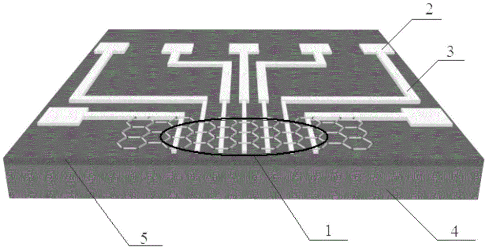
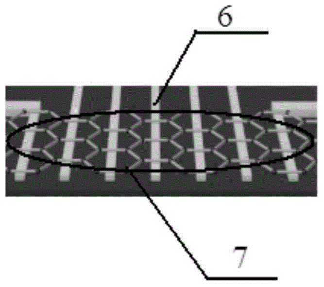
[0029] refer to figure 1 and figure 2 Shown, the structure of graphene field effect transistor biosensor: comprise base layer, described base layer is made of silicon substrate (6) and the silicon dioxide (7) that is deposited on the silicon substrate, is provided with sensing array on the base layer (1), electric pad (2) and wire (3), described sensing array comprises 7 parallel metal electrodes (4), and every two metal electrodes that are adjacent in sequence are combined to form a group of metal electrode pairs, altogether 6 groups of metal electrode pairs are formed, a graphene conductive channel (5) is formed by covering graphene between two metal electrodes of each group of metal electrode pairs, and each of the 7 metal electrodes is connected to an electric pad through a wire. connected, the electric pad is connected with the external signal detection device.

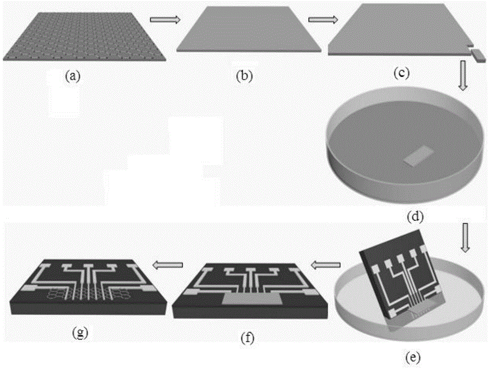
[0030] The preparation method of above-mentioned graphene field effect transistor biosensor, comprises the ...


PUM


Abstract

The invention belongs to a preparation method of a biosensor, and relates to a preparation method of a graphene field-effect transistor biosensor. The preparation method comprises the following steps: (1) preparing a single-layer graphene copper plate; (2) preparing devices on a substrate layer of a sensor; (3) performing directional transfer on graphene; and (4) heating to bake the sensor, removing PMMA (polymethyl methacrylate) with acetone, performing vacuum annealing, and modifying the graphene with probes to obtain the graphene field-effect transistor biosensor. According to the preparation method provided by the invention, large-scale preparation of the biosensor based on CVD (chemical vapor deposition) graphene can be realized, the copper etching time is short, and the preparation method is simple and quick and can greatly lower the manufacturing cost; and in the preparation process, the PMMA polymer is used only once (in the traditional method, the PMMA polymer is used for more times, at least three times), thus greatly improving the surface cleanliness of the graphene, retaining the intrinsic high performance of the graphene and being more beneficial to subsequent probe modification.

Description

technical field [0001] The invention belongs to a preparation method of a biosensor, in particular to a preparation method of a graphene field effect transistor biosensor. Background technique [0002] The development of modern medical technology is changing with each passing day, and the development of equipment technology provides the possibility for the application of various medical technologies in practice. Although the detection equipment used in clinical practice is highly integrated and automated, there are still many limitations, such as large equipment volume, high detection cost, low detection sensitivity and accuracy. Therefore, it is imperative to develop a micro-nano biosensor capable of real-time detection, high sensitivity, high specificity, label-free, and economical. In recent years, scientists from all over the world have found that field-effect transistor biosensors based on nanomaterials can meet various clinical requirements and make up for relevant li...

Claims


Application Information

Patent Timeline
Patent Type & Authority Applications(China)
IPC IPC(8): G01N27/414
Inventor 张国军郑超
Owner HUBEI UNIV OF CHINESE MEDICINE
Why Eureka
Try Eureka