PECVD coating and sintering process for protecting crystalline silicon solar cell against LID and PID

A technology of solar cells and solar cells, applied in circuits, photovoltaic power generation, electrical components, etc., can solve the problems of immaturity, poor compatibility of p-type production lines, restrictions on industrialization promotion, etc., and reduce the attenuation of conversion efficiency , fast and stable regeneration and recovery, and the effect of saving equipment costs

Active Publication Date: 2015-04-22
HENGDIAN GRP DMEGC MAGNETICS CO LTD
View PDF4 Cites 25 Cited by
  • Summary
  • Abstract
  • Description
  • Claims
  • Application Information

AI Technical Summary

Problems solved by technology

At present, the methods to solve LID mainly focus on the optimization and control of raw materials and silicon wafers, such as: (1) using high-resistivity silicon wafers, preparing silicon wafers by MCZ method or zone melting method to reduce their boron or oxygen content; 2) Use gallium-doped p-type silicon wafers or phosphorus-doped n-type silicon w

Method used


Image

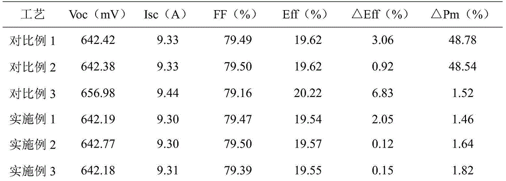
  • PECVD coating and sintering process for protecting crystalline silicon solar cell against LID and PID
  • PECVD coating and sintering process for protecting crystalline silicon solar cell against LID and PID

Examples


Embodiment 1

[0045] After sorting the silicon wafers, perform rough polishing in an alkaline solution (NaOH solution) to remove impurities and damaged layers, and obtain rough polished silicon wafers;

[0046] Put the roughly polished silicon wafer in an alkaline solution (NaOH solution) for texture, then wash and dry it, and the size of the texture is ≤5 μm;

[0047] The dried silicon wafer is placed in a diffusion furnace for high-temperature phosphorus diffusion, and after the PN junction is formed, the edge junction is removed by plasma etching and the PSG is removed by secondary cleaning. The square resistance of the emission area is 80ohm / squ;

[0048] Then perform PECVD coating on the silicon wafer: by deposition (passing SiH at the same time 4 and N 2 O) SiO is formed on the surface of the emission region x thin film, SiO x The film thickness is 10-20nm, the refractive index is 1.5; forming SiO x After thin film, continue to deposit to form SiN x / SiN y AR layer, SiO x Thin ...

Embodiment 2

[0051] After sorting the silicon wafers, perform rough polishing in an alkaline solution (NaOH solution) to remove impurities and damaged layers, and obtain rough polished silicon wafers;

[0052] Put the roughly polished silicon wafer in an alkaline solution (NaOH solution) for texture, then wash and dry it, and the size of the texture is ≤5 μm;

[0053] The dried silicon wafer is placed in a diffusion furnace for high-temperature phosphorus diffusion, and after the PN junction is formed, the edge junction is removed by plasma etching and the PSG is removed by secondary cleaning. The square resistance of the emission area is 80ohm / squ;

[0054] Then perform PECVD coating on the silicon wafer: by deposition (passing SiH at the same time 4 and N 2 O) SiO is formed on the surface of the emission region x thin film, SiO x The film thickness is 10-20nm, the refractive index is 1.5; forming SiO x After thin film, continue to deposit to form SiN x / SiN y AR layer, SiO x Thin ...

Embodiment 3

[0057] After sorting the silicon wafers, perform rough polishing in an alkaline solution (NaOH solution) to remove impurities and damaged layers, and obtain rough polished silicon wafers;

[0058] Put the roughly polished silicon wafer in an alkaline solution (NaOH solution) for texture, then wash and dry it, and the size of the texture is ≤5 μm;

[0059] The dried silicon wafer is placed in a diffusion furnace for high-temperature phosphorus diffusion, and after the PN junction is formed, the edge junction is removed by plasma etching and the PSG is removed by secondary cleaning. The square resistance of the emission area is 80ohm / squ;

[0060] Then perform PECVD coating on the silicon wafer: by deposition (passing SiH at the same time 4 and N 2 O) SiO is formed on the surface of the emission region x thin film, SiO x The film thickness is 10-20nm, the refractive index is 1.5; forming SiO x After thin film, continue to deposit to form SiN x / SiN y AR layer, SiO x Thin ...


PUM

PropertyMeasurementUnit
Film thicknessaaaaaaaaaa
Layer thicknessaaaaaaaaaa
Refractive indexaaaaaaaaaa

Abstract

The invention discloses a PECVD coating and sintering process for protecting a crystalline silicon solar cell against LID and PID, and belongs to the field of crystalline silicon solar cell manufacturing. The process comprises the steps that a silicon wafer is roughly polished, textured, cleaned and then spin-dried, wherein the size of the textured surface of the textured silicon wafer is smaller than or equal to 5 micrometers; high-temperature phosphorus diffusion is carried out, and etching is carried out after an emitter region is formed, wherein the square resistance of the emitter region ranges from 70 ohm/squ to 120 ohm/squ; after secondary cleaning, front surface PECVD coating, back electrode silk-screen printing and sintering and positive electrode silk-screen printing and sintering are carried out, and then manufacturing of the crystalline silicon solar cell is completed. By optimizing the PECVD coating process, the high-temperature sintering process and the regeneration and recovery process and controlling the concentration and diffusive motion of hydrogen atoms in crystalline silicon, suppression and improvement on LID of the crystalline silicon solar cell are achieved; meanwhile, by utilizing an SiOx film formed through deposition or plasma oxidation, PID of the crystalline silicon solar cell is effectively prevented, and the process can be applied to industrial production.

Description

technical field [0001] The invention belongs to the field of manufacturing crystalline silicon solar cells, in particular to a PECVD coating and sintering process for resisting light-induced degradation (LID) and potential-induced degradation (PID) of crystalline silicon solar cells. Background technique [0002] Due to the formation of boron-oxygen complexes under light, the LID phenomenon occurs, and the power attenuation of boron-doped p-type cells can be as high as 5%. For the p-type high-efficiency cell structure-PERC (passivated emitter Surface battery) technology, because its efficiency improvement is due to the improvement of the back passivation and back reflection performance of the battery sheet, the existence of the boron-oxygen compound hinders the migration of carriers to the back surface, which greatly swallows the power improvement brought by the high-efficiency battery structure. As a result, the PERC high-efficiency structure has more serious efficiency att...

Claims


Application Information

Patent Timeline
IPC IPC(8): H01L31/18H01L31/0216
CPCH01L31/1804H01L31/1864Y02E10/547Y02P70/50
Inventor 陈健生董方赵锋徐君傅晓敏包大新
Owner HENGDIAN GRP DMEGC MAGNETICS CO LTD
Why Eureka
Try Eureka