Distortion and noise cancellation based high-linearity CMOS broadband low noise amplifier

A broadband low-noise and noise-cancelling technology, applied in the direction of improving amplifiers to reduce noise impact and improving amplifiers to reduce nonlinear distortion, etc., can solve problems such as limited Q value, can not meet narrowband matching well, and achieve power consumption Low cost, convenient wireless multi-interface connection, and the effect of reducing costs

Inactive Publication Date: 2015-04-22
TIANJIN UNIV
View PDF3 Cites 7 Cited by
  • Summary
  • Abstract
  • Description
  • Claims
  • Application Information

AI Technical Summary

Problems solved by technology

The amplifier circuit does not use inductance, which avoids the problem that the narrow-band matching and frequency selection requirements cannot be well met due to the limited Q value.

Method used


Image

  • Distortion and noise cancellation based high-linearity CMOS broadband low noise amplifier
  • Distortion and noise cancellation based high-linearity CMOS broadband low noise amplifier
  • Distortion and noise cancellation based high-linearity CMOS broadband low noise amplifier

Examples


Embodiment

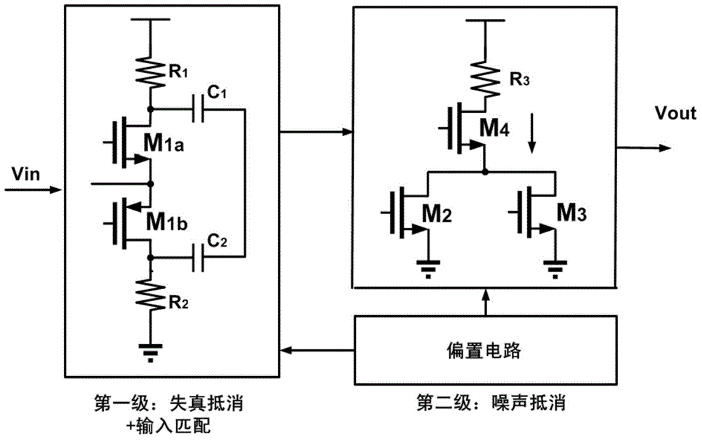
[0056] This embodiment adopts Figure 4 The circuit structure shown is based on the CHRT 0.18μm RFCMOS 1P6M process, and is simulated using the Cadence SpectreRF tool. The power supply voltage VDD is 1.8V, and the working frequency range is 0.1-1.6GHz.

[0057] For a standard RF system of 50Ω, the input impedance of the CMOS broadband low-noise amplifier LNA should satisfy (gm1a+gm1b)=20ms. Compared with a single NMOS common-gate stage, this structure can save nearly half of the bias current.

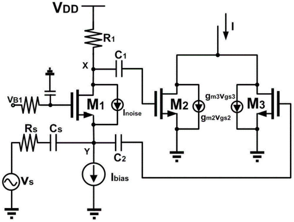
[0058] use Figure 5 The bias circuit biases M2 and M3 at 0.55V and 0.6V, respectively. Resistors R1 and R2 take values ​​of 500Ω and 480Ω respectively. For the convenience of S22 test, the resistance R3 is 50Ω.

[0059] Image 6 The simulation result diagram of S parameters is given, where S11, S12 and S22 represent the input reflection coefficient, reverse transmission coefficient and output reflection coefficient respectively. From the simulation results, it has good input match...


PUM


Abstract

The invention discloses a distortion and noise cancellation based high-linearity CMOS broadband low noise amplifier. The distortion and noise cancellation based high-linearity CMOS broadband low noise amplifier structurally comprises a distortion cancellation input stage and a noise cancellation output stage. The distortion cancellation input stage serves as a first stage of the low noise amplifier, input impedance matching and second-order cross modulation IMD2 cancellation are achieved by adopting CMOS complementary common-gate combination, meanwhile a complementary structure has the characteristic of current reuse, and accordingly power consumption is reduced. The noise cancellation output stage serves as a second stage and is mainly used for cancelling channel thermal noise current of two common-gate devices at the first stage and accordingly reducing the noise coefficient of a whole circuit. The distortion and noise cancellation based high-linearity CMOS broadband low noise amplifier can simultaneously achieve high linearity and low noise coefficient within a broadband range, and meanwhile gives consideration to other design parameters, such as input impedance matching, power gain and power consumption.

Description

technical field [0001] The invention belongs to the technical field of radio frequency integrated circuits, and in particular relates to a CMOS broadband low-noise amplifier (LNA) which simultaneously adopts distortion and noise canceling technologies. Background technique [0002] With the continuous emergence of mobile communication technologies such as 3G / 4G, wireless transceiver technology represented by radio frequency microwave is developing unprecedentedly. Different from the mature second-generation mobile communication devices, the current mobile communication terminals are tending to integrate multiple communication standards to meet the seamless connection of the network to realize real-time sharing of information. For example, smart phones can use GSM, WCDMA, WIFI and RFTV Wait. Traditional solutions are based on paralleling multiple narrowband paths to achieve multi-standard communication. This solution often occupies a large chip area and has stability problem...

Claims


Application Information

Patent Timeline
IPC IPC(8): H03F1/26H03F1/32
Inventor 秦国轩屠国平杨来春闫月星
Owner TIANJIN UNIV
Why Eureka
Try Eureka