TDC-based high-speed column level ADC for imaging sensor

An image sensor, high-speed technology, applied in the electrical field, which can solve the problems of limiting the readout rate of CMOS image sensors, column-level fixed pattern noise, etc.

Inactive Publication Date: 2015-04-22
TIANJIN UNIV
View PDF5 Cites 7 Cited by
  • Summary
  • Abstract
  • Description
  • Claims
  • Application Information

AI Technical Summary

Problems solved by technology

[0005] (2) Mismatch between columns in the column-level A / D converter will introduce column-level fixed pattern noise
It can be seen that with the improvement of conversion accuracy, the conversion time increases exponentially, which greatly limits the readout rate of CMOS image sensors.

Method used


Image

  • TDC-based high-speed column level ADC for imaging sensor
  • TDC-based high-speed column level ADC for imaging sensor
  • TDC-based high-speed column level ADC for imaging sensor

Examples


Embodiment Construction
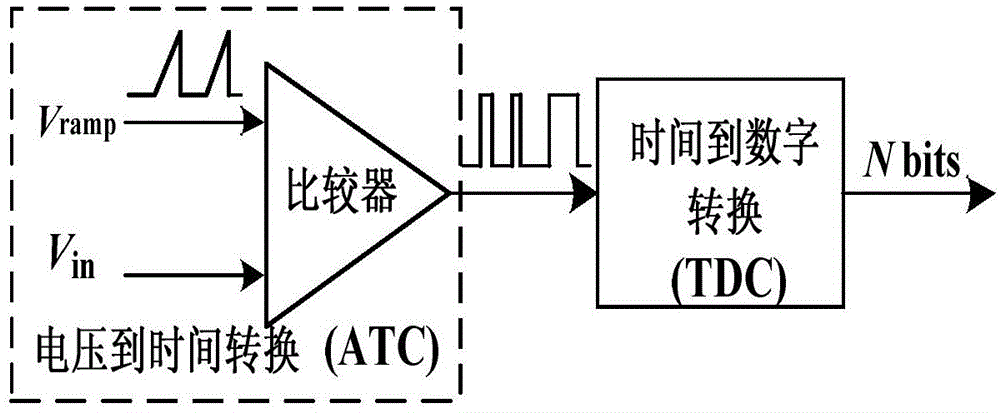
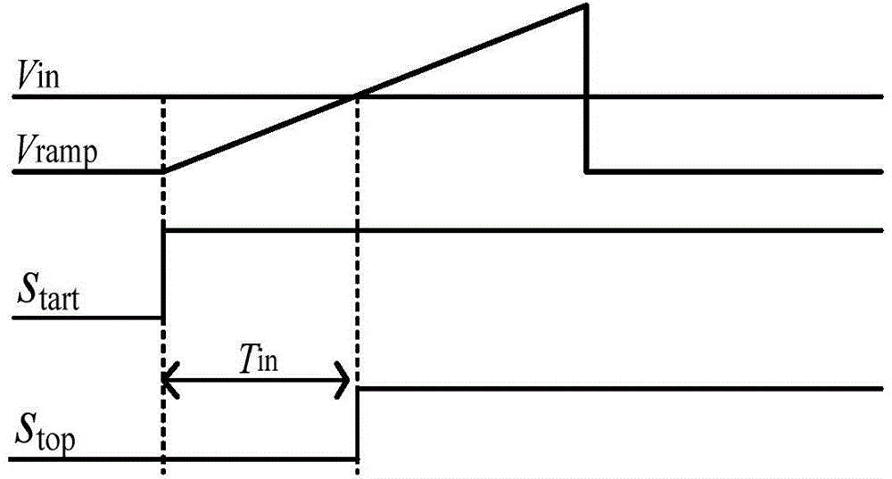
[0023] The basic idea of ​​the present invention is to use time to digital conversion (TDC) technology to divide the conversion process from analog to digital into two parts, figure 1 It is an overall architecture diagram of the present invention. The first part is the conversion of analog to time (ATC), which is composed of a ramp generator and a comparator, which can convert the input analog voltage into a proportional time amount, and its timing is as follows figure 2 shown. At the beginning of the ramp signal, a start pulse signal Start is generated. When the input voltage is equal to the voltage of the ramp signal, the comparator is reversed to obtain a stop pulse signal Stop, and the quantized time interval Tin is equivalent to two signals of Start and Stop. delay difference between. The second part uses TDC to quantify the time interval width to complete the conversion from time to digital.

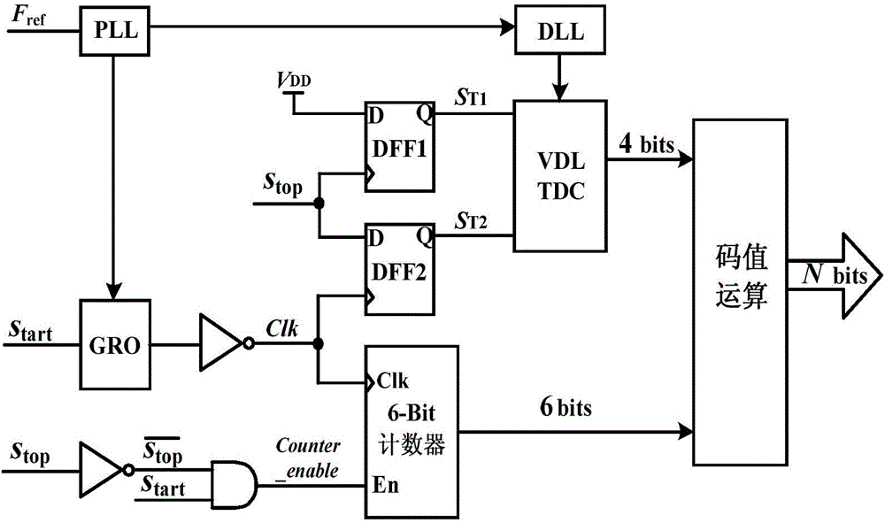
[0024] image 3 It shows the overall structure of TDC, which consists of ...


PUM


Abstract

The invention belongs to the field of analog-digital conversion circuits. For the CIS with a large pixel array or high scanning speed, in order to reducing conversion time of a column level single-slope ADC under the condition that the area and power consumption are not greatly increased, the adopted technical scheme is that a TDC-based high-speed column level ADC for an imaging sensor is provided. The TDC-based high-speed column level ADC is composed of a phase-locked loop circuit PLL, a gating ring oscillator GRO, two phase inverters, an AND gate circuit, two D triggers, a counter, a delayed phase-locked loop circuit DLL, a vernier delay line VDL and a code value arithmetic unit. The TDC-based high-speed column level ADC for the imaging sensor is mainly applied to analog-digital conversion devices.

Description

technical field [0001] The invention belongs to the electrical field and relates to an analog-to-digital conversion, in particular to the realization of a column-level ADC applied in an image sensor. Specifically, TDC-based high-speed column-level ADCs for image sensors technical background [0002] With the rapid development of digital technology and semiconductor manufacturing technology, CMOS image sensor (CIS) has become the object of current and future market attention. At present, there are three main architectures of analog-to-digital converters (ADCs) used in CMOS image sensors: chip level, pixel level, and column-parallel level. On-chip ADCs use one ADC for the entire pixel array, so the ADC must be very fast to achieve a high frame rate. Pixel-level ADCs place an ADC in each pixel to achieve extremely high frame rates, but this comes at the expense of silicon area and power consumption. The array-level ADC is converted by an ADC for each column, so as to achieve...

Claims


Application Information

Patent Timeline
Patent Type & Authority Applications(China)
IPC IPC(8): H04N5/3745H04N5/378H04N1/031
Inventor 徐江涛于婧聂凯明高静高志远史再峰姚素英
Owner TIANJIN UNIV
Why Eureka
Try Eureka