Metal oxide semiconductor gas sensor and preparation method thereof

A technology of oxide semiconductors and gas sensors, which is applied in the direction of instruments, scientific instruments, measuring devices, etc., can solve the problems of sensor sensitivity drop, sensor body resistance drift, and reduce the service life of sensors, so as to prevent drift, improve service life, and high The effect of detection accuracy

Active Publication Date: 2015-04-29
苏州纳格传感技术有限公司
View PDF8 Cites 34 Cited by
  • Summary
  • Abstract
  • Description
  • Claims
  • Application Information

AI Technical Summary

Problems solved by technology

However, due to the easy introduction of other impurities or other incompletely reacted crystal phases during the chemical preparation process, there may be voids or other defects in the sensitive material, and these defects will further lead to the drift of the bulk resistance of the sensor during long-term service, resulting in sensor Sensitivity decreases, which in turn reduces the service life of the sensor

Method used


Image

  • Metal oxide semiconductor gas sensor and preparation method thereof
  • Metal oxide semiconductor gas sensor and preparation method thereof
  • Metal oxide semiconductor gas sensor and preparation method thereof

Examples


Embodiment 1

[0068] Prepare the nickel oxide bulk resistance layer as the first film layer by magnetron sputtering, control the coating time and coating power, so that the thickness of the nickel oxide bulk resistance layer is 600nm, the cross-sectional electron microscope diagram of the obtained nickel oxide bulk resistance layer is as follows Figure 5 As shown, the surface electron microscope image is shown in Image 6 As shown; then the nickel oxide nanowall was prepared as the second film layer by chemical water bath deposition method, and the coating time was controlled so that the thickness of the nanowall was 1 μm, and a formaldehyde gas sensor with a double-layer detection layer was obtained. The formaldehyde gas sensor in this embodiment shows good gas-sensing characteristics to formaldehyde gas, and the specific corresponding characteristic diagram is as follows Figure 7 shown.

Embodiment 2

[0070] The nickel oxide body resistance layer was prepared by magnetron sputtering as the first film layer, and the coating time and coating power were controlled so that the thickness of the nickel oxide body resistance layer was 350nm; then the nickel oxide nanowall was prepared by chemical water bath deposition as the second film layer. Thin film layer, control the water bath deposition time, so that the thickness of the nano wall is 1.5 μm, and the formaldehyde gas sensor with the double-layer structure of the detection layer is obtained, wherein the cross-sectional electron microscope diagram of the detection layer is as follows Figure 8 As shown, the surface electron microscope image is shown in Figure 9 shown. from Figure 8 with Figure 9 It can be seen from the comparison that the second thin film layer located on the surface obviously has a larger specific surface area than the first thin film layer.

Embodiment 3

[0072] A nickel oxide bulk resistive layer was prepared by laser pulse deposition as the first film layer, and the coating time and laser power were controlled so that the thickness of the nickel oxide bulk resistive layer was 1 μm; nickel oxide nanowires were then prepared by electrospinning as the second thin film layer, and the spinning time was controlled so that the thickness of the nanowires was 50 μm, and a formaldehyde gas sensor with a double-layer detection layer was prepared. As a comparison with Example 2, the response of the gas sensor in formaldehyde gas when the nickel oxide nanowire sensitive layer is not provided is as follows: Figure 10 As shown, there is only a weak response under high concentration of formaldehyde gas.


PUM

PropertyMeasurementUnit
thicknessaaaaaaaaaa
thicknessaaaaaaaaaa
thicknessaaaaaaaaaa

Abstract

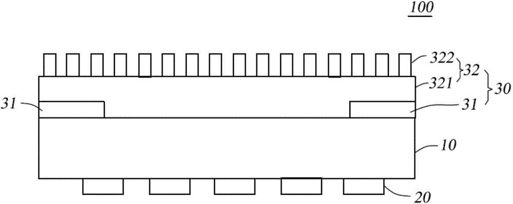
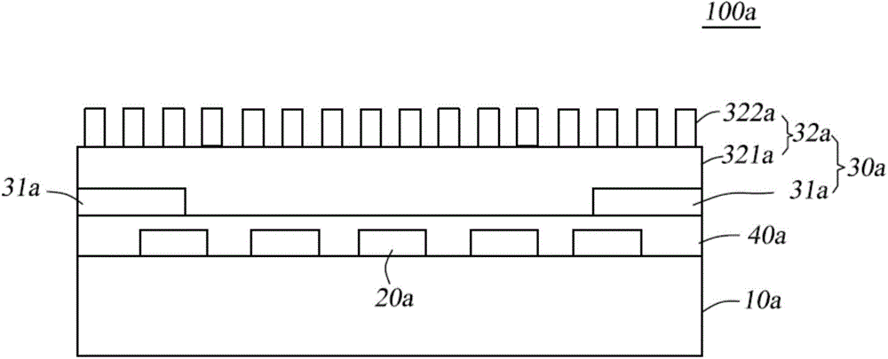
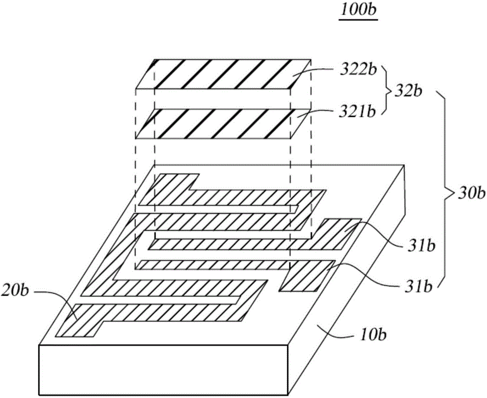
The invention discloses a metal oxide semiconductor gas sensor and a preparation method thereof. The semiconductor gas sensor comprises a substrate, a heating layer which is arranged on the substrate, a functional layer which is arranged on the substrate and insulated from the heating layer, wherein the functional layer comprises a signal electrode and a detection layer which are electrically connected with each other; the detection layer comprises a first film layer and a second film layer which are sequentially formed on the substrate; the first film layer is smaller than the second film layer in specific surface area. According to the semiconductor gas sensor disclosed by the invention, the detection layer is configured to comprise the first film layer and the second film layer which are different in specific surface area; the first film layer which is smaller in specific surface area is taken as a bulk resistor layer for stabilizing bulk resistance and preventing excursion of the bulk resistance of the detection layer; the second film layer which is larger in specific surface area is taken as a gas sensitive layer for detecting target gas, so that the service life of the semiconductor gas sensor is prolonged and relatively high detection precision is guaranteed.

Description

technical field [0001] The invention belongs to the technical field of electronic device manufacturing, and in particular relates to a semiconductor gas sensor and a preparation method thereof. Background technique [0002] With the rapid development of industry, the problem of environmental pollution is becoming more and more serious. For example, CO and NO in automobile exhaust x , SO x Harmful gases such as formaldehyde and toluene in interior decoration, methane gas leaked from coal mines, flammable, explosive and toxic gases produced in chemical production, etc. These toxic gases pose a serious threat to people's health . In order to ensure personal safety and prevent problems before they happen, various detection methods and detection instruments have been developed. Among them, gas sensors play an important role in the fields of home life, emission monitoring, aviation, medical treatment, and sanitation. [0003] At present, there are many kinds of gas sensors with...

Claims


Application Information

Patent Timeline
Patent Type & Authority Applications(China)
IPC IPC(8): G01N27/00
Inventor 张克栋顾唯兵王玲崔铮
Owner 苏州纳格传感技术有限公司
Why Eureka
Try Eureka