Organic electroluminescent component and manufacturing method thereof

An electroluminescent device and luminescent technology, which is applied in the direction of electric solid-state devices, semiconductor/solid-state device manufacturing, electrical components, etc., can solve the problem of low luminous efficiency

Inactive Publication Date: 2015-04-29
OCEANS KING LIGHTING SCI&TECH CO LTD +2
View PDF0 Cites 5 Cited by
  • Summary
  • Abstract
  • Description
  • Claims
  • Application Information

AI Technical Summary

Problems solved by technology

[0004] Based on this, it is necessary to provide an organic electroluminescent device with high luminous efficiency for the problem of low luminous efficiency of general organic electroluminescent devices

Method used


Image

  • Organic electroluminescent component and manufacturing method thereof
  • Organic electroluminescent component and manufacturing method thereof
  • Organic electroluminescent component and manufacturing method thereof

Examples


preparation example Construction

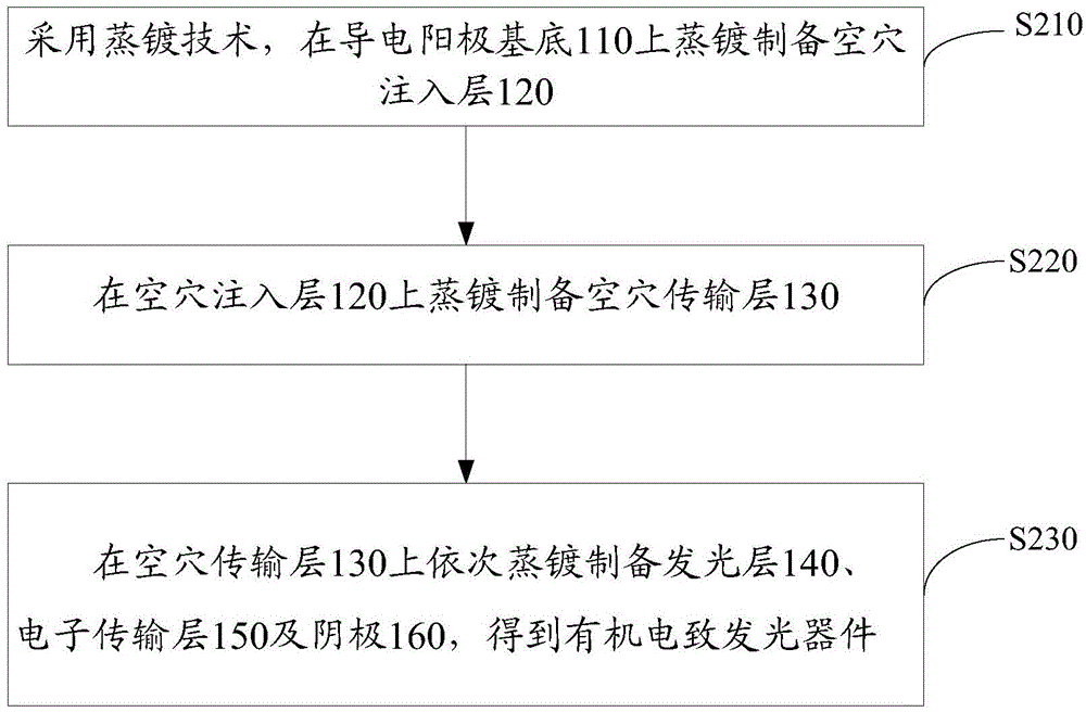
[0046] see figure 2 , the preparation method of the organic electroluminescent device of an embodiment, comprises the following steps:

[0047] S210 , preparing a hole injection layer 120 on the conductive anode substrate 110 by evaporation using an evaporation technique.

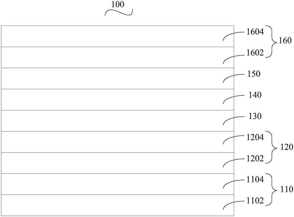
[0048] Wherein, the conductive anode substrate 110 includes a transparent substrate 1102 and an anode layer 1104 prepared on the transparent substrate 1102 . Preferably, the transparent substrate 1102 is glass. The material of the anode layer 1104 is indium tin oxide (ITO). The sheet resistance of the anode layer 1104 is 5˜100Ω / sq.

[0049] The hole injection layer 120 includes a first hole injection auxiliary layer 1202 stacked on the anode layer 1104 and a second hole injection auxiliary layer 1204 stacked on the first hole injection auxiliary layer 1202 .

[0050] The material of the first hole injection auxiliary layer 1202 is copper oxide (CuO), cuprous oxide (Cu 2 O), copper fluoride (CuF 2 ) o...

Embodiment 1

[0079] The structure of the organic electroluminescent device prepared in this embodiment is: ITO / CuF 2 / NiO / NPB / NPB:Ir(MDQ) 2 (acac) / Bphen / LiF / Ag; wherein, the oblique bar " / " indicates a layered structure, and the colon ":" indicates doping, the same below.

[0080] The preparation of the organic electroluminescent device of this embodiment is as follows:

[0081] (1) Wash the ITO glass substrate sequentially with detergent, deionized water, and ultrasonic for 15 minutes to remove organic pollutants on the glass surface. The square resistance of the ITO conductive glass is 5Ω / sq.

[0082] (2) The first hole injection auxiliary layer and the second hole injection auxiliary layer were sequentially evaporated on the surface of the ITO glass substrate.

[0083] The material of the first hole injection auxiliary layer is CuF 2 , with a thickness of 1 nm. The first hole injection auxiliary layer is prepared by electron beam evaporation technology, and the working pressure is 1...

Embodiment 2

[0095] The structure of the organic electroluminescent device prepared in this example is: ITO / CuO / NiO / MeO-TPD / Alq 3 :DCJTB / TPBi / CsF / Al.

[0096] The preparation of the organic electroluminescent device of this embodiment is as follows:

[0097] (1) Wash the ITO glass substrate sequentially with detergent, deionized water, and ultrasonic for 15 minutes to remove organic pollutants on the glass surface. The square resistance of the ITO conductive glass is 100Ω / sq.

[0098] (2) The first hole injection auxiliary layer and the second hole injection auxiliary layer were sequentially evaporated on the surface of the ITO glass substrate.

[0099] The material of the first hole injection auxiliary layer is CuO, and the thickness is 5 nm. The first hole injection auxiliary layer is prepared by electron beam evaporation technology, and the working pressure is 1×10 -3 Pa, the evaporation rate is 0.1nm / s.

[0100] The material of the second hole injection auxiliary layer is NiO, and ...


PUM


Abstract

An organic electroluminescent component comprises a conductive anode substrate, and a hole injection layer, a hole transmission layer, a luminescent layer, an electron transmission layer and a cathode which are sequentially laminated on an anode layer of the conductive anode substrate, wherein the hole injection layer comprises a first hole injection auxiliary layer laminated on the anode layer and a second hole injection auxiliary layer laminated on the first hole injection auxiliary layer; the first hole injection auxiliary layer is made of copper oxide, cuprous oxide, copper fluoride or cuprous fluoride; the second hole injection auxiliary layer is made of nickel oxide. The organic electroluminescent component uses two hole injection auxiliary layers, so that the hole injection efficiency is improved and further the luminescent efficiency of the organic electroluminescent component is improved. The invention further provides a manufacturing method of the organic electroluminescent component.

Description

technical field [0001] The invention relates to the field of organic electroluminescent devices, in particular to an organic electroluminescent device and a preparation method thereof. Background technique [0002] Organic Light Emission Diode, hereinafter referred to as OLED, has the characteristics of high brightness, wide range of material selection, low driving voltage, fully cured active light emission, etc., and has the advantages of high definition, wide viewing angle, and fast response speed. It is a display technology and light source with great potential, which conforms to the development trend of mobile communication and information display in the information age, as well as the requirements of green lighting technology, and is the focus of many researchers at home and abroad. [0003] Although researchers from all over the world have greatly improved various indicators of device performance by selecting appropriate organic materials and rational device structure ...

Claims


Application Information

Patent Timeline
Patent Type & Authority Applications(China)
IPC IPC(8): H01L51/52H01L51/54H01L51/56
CPCH10K50/17H10K71/00
Inventor 周明杰冯小明钟铁涛王平
Owner OCEANS KING LIGHTING SCI&TECH CO LTD
Why Eureka
Try Eureka