
A kind of nitride high electron mobility transistor epitaxial structure and preparation method thereof

A technology with high electron mobility and epitaxial structure, applied in semiconductor/solid-state device manufacturing, circuits, electrical components, etc., can solve the problem of destroying surface morphology, deteriorating GaN/InAlN interface quality, and reducing channel two-dimensional electron gas transport characteristics and other issues, to avoid damage and improve the effect of transport characteristics

Inactive Publication Date: 2017-11-07
NO 55 INST CHINA ELECTRONIC SCI & TECHNOLOGYGROUP CO LTD
View PDF3 Cites 0 Cited by
  • Summary
  • Abstract
  • Description
  • Claims
  • Application Information

AI Technical Summary

Problems solved by technology

Therefore, before growing the GaN channel after the InAlN barrier is grown, a temperature rise process must be carried out. The temperature rise will cause the volatilization of In atoms on the InAlN surface, thereby destroying the surface morphology, deteriorating the quality of the GaN / InAlN interface, and reducing the two-dimensional electron density of the channel. Transport properties of gas

Method used


Image

  • A kind of nitride high electron mobility transistor epitaxial structure and preparation method thereof

Examples


Embodiment 1

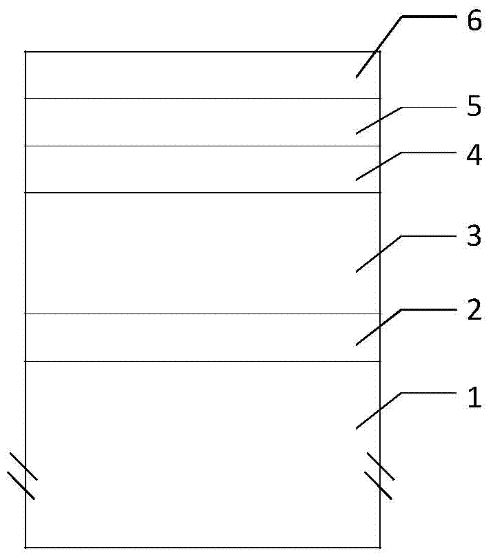
[0023] 1) Select the C-plane SiC substrate and grow it by MOCVD technology;

[0024] 2) Baking at 1080°C and 100Torr in a hydrogen atmosphere for 10 minutes;

[0025] 3) At 1100°C, inject ammonia gas and trimethylaluminum, and grow a 50nm thick AlN nucleation layer on the substrate surface;

[0026] 4) Introduce ammonia gas and trimethylgallium to grow a 2um thick N-polar GaN buffer layer;

[0027] 5) Turn off trimethylgallium, lower the temperature to 780°C, turn on trimethylaluminum and trimethylindium, and grow the first InAlN barrier layer with a thickness of 20nm and a constant In composition of 0.18;

[0028] 6) Keep the flow rate of trimethylaluminum and trimethylindium constant, and gradually increase the growth temperature to 1050°C, and at the same time grow InAlN with a thickness of 15nm and a gradient composition, which is the second barrier layer;

[0029]7) At 1050°C, turn off trimethylaluminum and trimethylindium, turn on trimethylgallium, and grow a 20nm thic...


PUM


Abstract

The invention discloses a nitride high electron mobility transistor epitaxial structure and a preparation method thereof. The nitride high electron mobility transistor epitaxial structure includes a substrate layer on which a core layer, a buffer layer, a barrier layer and a channel layer are sequentially grown on the substrate layer from the bottom up, wherein the substrate layer is sapphire or SiC; the core layer is AlN, GaN or AlGaN; the buffer layer is GaN, and the channel layer is GaN; the barrier layer is a composite InAlN barrier including two layers of structures, the first layer is InAlN with constant common components (the In component is a value within 0.16-0.19, and lattice-matched with GaN), the second layer is InAlN with gradually changed components, and the In component is gradually changed from a value within 0.16-0.19 to zero from the bottom up. According to the nitride high electron mobility transistor epitaxial structure and the preparation method thereof, the damage to a heterojunction interface is avoided, and the transport characteristics of two-dimensional electron gas is improved; compared with the InAlN barrier layer with constant common components, the In component of the InAlN barrier layer is gradually changed to be zero from the bottom up, so that the InAlN alloy is gradually changed to be AlN with stronger polarization effect, and thereby the electron concentration of the channel can be further improved.

Description

technical field [0001] The invention belongs to the technical field of semiconductor single crystal thin films, and in particular relates to a nitride high electron mobility transistor epitaxial structure of an InAlN barrier layer and a preparation method thereof. Background technique [0002] Millimeter-wave power devices are key components of systems such as microwave communications. Gallium nitride (GaN)-based high electron mobility field-effect transistors (HEMTs), as the third-generation wide-bandgap compound semiconductor devices, have excellent characteristics of high frequency and high power , making it have an important application prospect in the field of microwave communication. [0003] As we all know, the gate length of the device is closely related to the frequency characteristics of the device. In the low frequency range, the frequency of the device is basically inversely proportional to the gate length; as the gate length shortens, especially when entering t...

Claims


Application Information

Patent Timeline
Patent Type & Authority Patents(China)
IPC IPC(8): H01L29/778H01L29/205H01L21/02
Inventor 彭大青李忠辉
Owner NO 55 INST CHINA ELECTRONIC SCI & TECHNOLOGYGROUP CO LTD
Learn More