High depth-to-width ratio super-resolution nano photoetching structure and method
A high-aspect-ratio, nano-lithography technology, which is applied in microlithography exposure equipment, photolithography exposure equipment, etc., can solve the problems of complex, expensive, and complex equipment for oblique incidence of light beams
- Summary
- Abstract
- Description
- Claims
- Application Information
AI Technical Summary
Problems solved by technology
Method used
Image

Examples
Embodiment Construction
[0033] The present invention will be further described below in conjunction with accompanying drawing and embodiment:
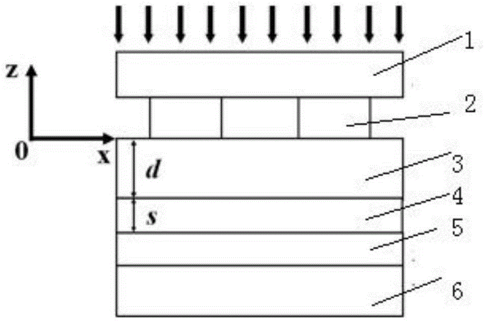
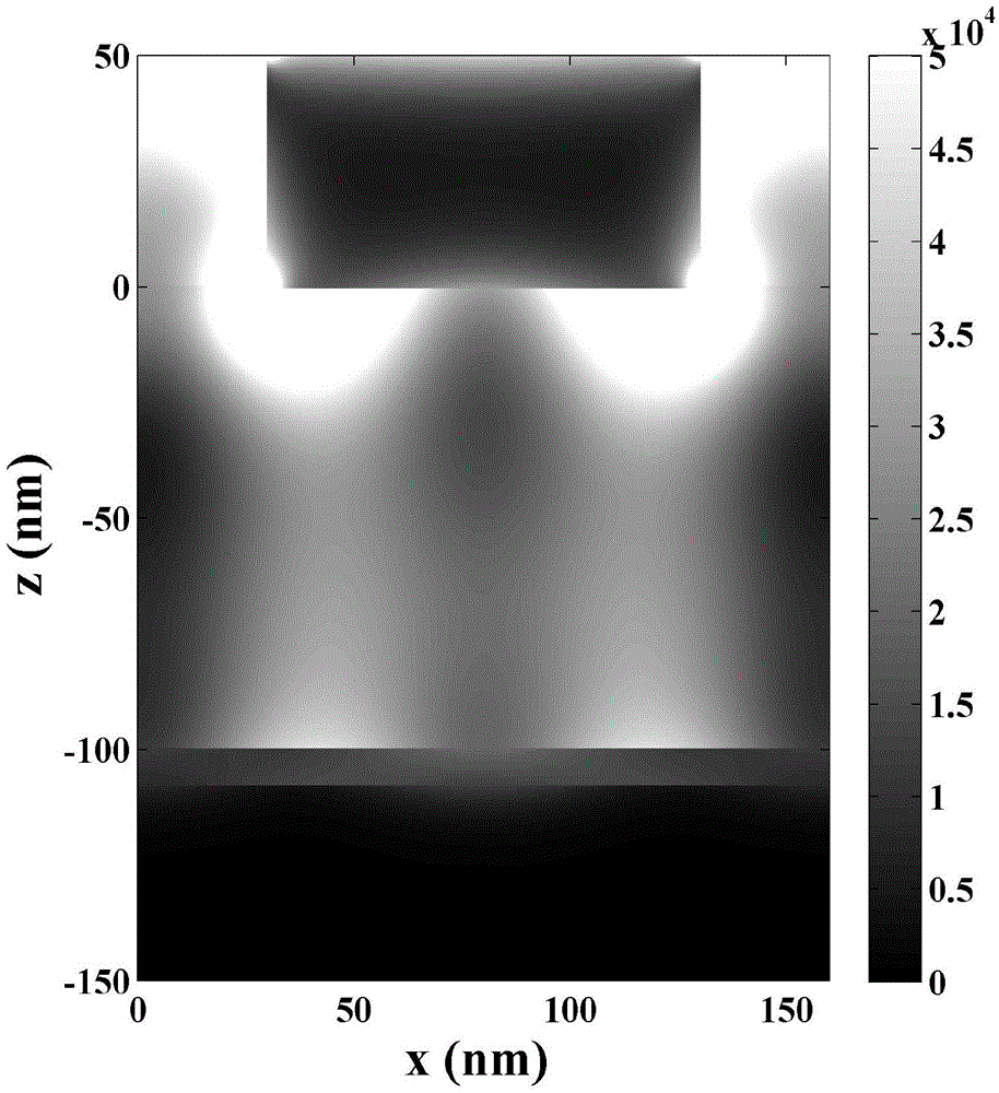
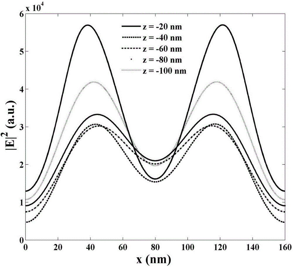
[0034] Such as figure 1 As shown, the high aspect ratio super-resolution nanolithography structure sequentially includes a transparent upper substrate layer 1, a metal grating layer 2, a photoresist layer 3, a gain medium layer 4, a metal thin film layer 5 and a lower substrate layer 6. The metal grating layer 2, the photoresist layer, the gain medium layer and the metal thin film layer together constitute a four-layer metal waveguide resonant cavity structure based on surface plasmons;
[0035] SiO 2 The formed upper base layer 1. The metal grating layer 2 is made of Cr, the underlying metal film layer 5 is made of Al, and the gain medium layer 4 is made of GaN. The incident P polarized light is vertically incident from top to bottom, the wavelength is 365nm, SiO 2 The refractive indices of photoresist and GaN are 1.4745, 1.7 and 2.6538, respectively, an...
PUM
| Property | Measurement | Unit |
|---|---|---|
| Thickness | aaaaa | aaaaa |
| Thickness | aaaaa | aaaaa |
Abstract
Description
Claims
Application Information
 - R&D
- Intellectual Property
- Life Sciences
- Materials
- Tech Scout
- Unparalleled Data Quality
- Higher Quality Content
- 60% Fewer Hallucinations
Browse by: Latest US Patents, China's latest patents, Technical Efficacy Thesaurus, Application Domain, Technology Topic, Popular Technical Reports.
© 2025 PatSnap. All rights reserved.Legal|Privacy policy|Modern Slavery Act Transparency Statement|Sitemap|About US| Contact US: help@patsnap.com