Encapsulation structure of fingerprint identification sensor and encapsulation method thereof

A technology of fingerprint identification and packaging structure, which is applied in character and pattern recognition, acquisition/organization of fingerprints/palmprints, instruments, etc. It can solve problems such as process troubles, thick glue, and impact on product reliability, and improve electrical insulation performance , Improve production efficiency and improve product reliability

Active Publication Date: 2015-05-13
JIANGYIN CHANGDIAN ADVANCED PACKAGING CO LTD
View PDF5 Cites 18 Cited by
  • Summary
  • Abstract
  • Description
  • Claims
  • Application Information

AI Technical Summary

Problems solved by technology

When only one layer of organic material is used as the insulating layer, the figure 1 There will be electrical connection problems in the upper corner I area of ​​the Trench trench, such as short circuit, open circuit, leakage current, etc., which will affect the reliability of the product; and when two layers of organic materials are used as the insulating layer, it will cause figure 1 The glue thickness in the lower corner II area of ​​the middle trench groove is thicker, causing troubles in subsequent processes (such as exposure and development)

Method used


Image

  • Encapsulation structure of fingerprint identification sensor and encapsulation method thereof
  • Encapsulation structure of fingerprint identification sensor and encapsulation method thereof
  • Encapsulation structure of fingerprint identification sensor and encapsulation method thereof

Examples


Embodiment

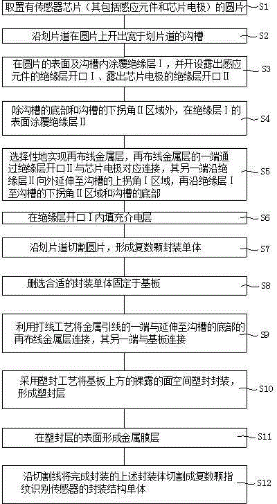
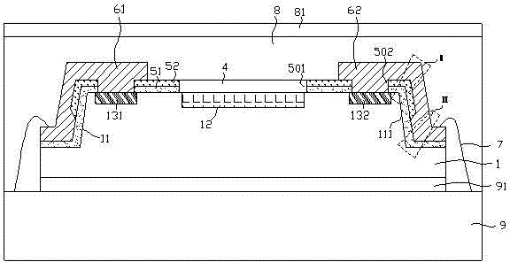
[0075] Examples, see image 3

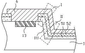
[0076] The packaging structure of a fingerprint identification sensor according to the present invention has a rectangular cross-section of the silicon base body 1 , and the sensor chip is arranged on the top of the silicon base body 1 , which includes an inductive element 12 and chip electrodes arranged around the inductive element 12 . Chip electrodes and related circuits are arranged inside the silicon base body 1 and shown on the top. In the figure, two electrodes 131 and 132 are taken as examples, and the upper surfaces of the electrodes 131 and 132 expose the silicon base body 1 . The sensing element 12 is embedded in the upper part of the silicon base body 1 between the two electrodes 131, 132, and the upper surface of the silicon base body 1 is exposed, and is used to measure the capacitance between the user's fingerprints, thereby obtaining an image of the customer's finger information. The number of chip electrodes can be more than t...


PUM


Abstract

The invention relates to an encapsulation structure of a fingerprint identification sensor and an encapsulation method thereof, and belongs to the technical field of semiconductor encapsulation. The encapsulation structure of the fingerprint identification sensor is characterized in that a groove is formed in the edge position of the top of a silicon substrate body, a sensor chip is arranged at the top of the silicon substrate body, and comprises a sensing element and chip electrodes arranged around the sensing element, an insulation layer I covers the surface of the silicon substrate body and an uncovered face of the groove, an insulation layer II covers the insulation layer I from the top down until an upper corner area I, a re-wiring metal layer enables electrode signals to drop to the bottom of the groove, a metal lead wire is connected with the re-wiring metal layer and a substrate, a dielectric layer is filled in an opening of the insulation layer I, a plastic seal layer seals all uncovered surface space of the silicon substrate body on the substrate, and a metal film layer is arranged on the surface of the plastic seal layer. The encapsulation structure of the fingerprint identification sensor can improve product insulating performance and reliability. The encapsulation method of the encapsulation structure of the fingerprint identification sensor uses a wafer level technology, is simple in encapsulation process, improves production efficiency, and conforms to a development trend of encapsulation industry.

Description

technical field [0001] The invention relates to a packaging structure of a fingerprint identification sensor and a packaging method thereof, belonging to the technical field of semiconductor packaging. Background technique [0002] With the development of the times, Trench (groove) technology has been widely used in the manufacturing process of existing semiconductor packaging structures, such as figure 1 As shown, in the packaging structure of the traditional fingerprint recognition sensor, the electrical connection between the sensor chip and the outside is to use metal wires to connect the I / O on the chip to the packaging carrier in a bonding manner and realize it through the packaging pins. The insulating layer of this structure usually has only one layer of organic material (such as figure 1 51) or two layers of organic materials (such as figure 1 51 and 52). When only one layer of organic material is used as the insulating layer, the figure 1 There will be electric...

Claims


Application Information

Patent Timeline
Patent Type & Authority Applications(China)
IPC IPC(8): G06K9/00H01L23/31H01L21/50
CPCH01L21/56H01L23/3192G06V40/1306H01L2924/10155H01L2224/48091H01L2224/73265H01L2924/00014
Inventor 龙欣江毕金栋郭亮徐虎高军明张黎陈栋郭洪岩梅万元章力陈锦辉赖志明
Owner JIANGYIN CHANGDIAN ADVANCED PACKAGING CO LTD
Why Eureka
Try Eureka