MEMS (Micro Electro Mechanical Systems) pressure sensor and formation method thereof

A pressure sensor and pressure technology, applied in the direction of measuring fluid pressure, measuring fluid pressure through electromagnetic components, instruments, etc., can solve the problems of difficult yield of integrated circuits, large device size, and reduced pressure sensor performance.

Active Publication Date: 2015-05-20
MEMSEN ELECTRONICS
View PDF6 Cites 13 Cited by
  • Summary
  • Abstract
  • Description
  • Claims
  • Application Information

AI Technical Summary

Problems solved by technology

[0006] In the existing manufacturing methods of MEMS pressure sensors, the process of integrating the pressure sensor chip and the signal processing circuit is quite different, and it is difficult to achieve monolithic integration.
At the same time, when the integrated circuit and the pressure sensor are fabricated on a single substrate, the existence of the pressure sensor has hindered the development of the integrated circuit, and the existence of the integrated circuit on the same substrate has also caused difficulties in the manufacture of small-sized pressure sensors.
Therefore, the manufacturing process of using a single substrate as an integrated circuit and a pressure sensor is more complicated, and the size of the formed device is larger, resulting in an increase in manufacturing cost
[0007] When making an integrated pressure sensor and circuit on a single substrate, if the components of the pressure sensor are made first, and then the circuit is made, the process of the pressure sensor often affects the substrate, resulting in a decrease in the yield of integrated circuits that is difficult to make
If the integrated circuit is made first, and then the pressure sensor is made, the existence of the integrated circuit has great restrictions on the choice of pressure sensor material and the temperature of the processing process, which will seriously reduce the performance of the pressure sensor

Method used


Image

  • MEMS (Micro Electro Mechanical Systems) pressure sensor and formation method thereof
  • MEMS (Micro Electro Mechanical Systems) pressure sensor and formation method thereof
  • MEMS (Micro Electro Mechanical Systems) pressure sensor and formation method thereof

Examples


Embodiment 1

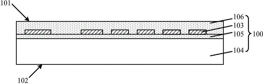
[0092] Figure 1 to Figure 9 It is a schematic cross-sectional structure diagram of the forming process of the MEMS pressure sensor according to an embodiment of the present invention.

[0093] Please refer to figure 1 , providing a first substrate 100, the first substrate 100 includes an opposite first surface 101 and a second surface 102, the first substrate 100 includes at least one conductive layer 103, and the conductive layer 103 is located at the The side of the first surface 101 of the first substrate 100 described above.

[0094] The first substrate 100 is used to form a conductive layer 103, and the conductive layer 103 is used to transmit the electrical signal output by the piezoresistive element on the second substrate. In this embodiment, the first substrate 100 further includes a circuit, and the conductive layer 103 may be a part of the conductive layer of the circuit, or may be an additional conductive layer on the circuit. The conductive layer 103 may inclu...

Embodiment 2

[0172] Figure 10 to Figure 11 It is a schematic cross-sectional structure diagram of the forming process of the MEMS pressure sensor according to another embodiment of the present invention.

[0173] Please refer to Figure 10 , providing a first substrate 200, the first substrate 200 includes an opposite first surface 201 and a second surface 202, the first substrate 200 includes at least one conductive layer 203, and the conductive layer 203 is located at the On the side of the first surface 201 of the first substrate 200 , the first substrate 200 further includes a self-test electrode 230 .

[0174] In addition, the first substrate 200 also includes a circuit, and the circuit includes a semiconductor device structure and an electrical interconnection structure. The conductive layer 203 may be a part of the conductive layer of the circuit, or an additional conductive layer on the circuit. . The conductive layer may include a conductor or a semiconductor.

[0175] In thi...

Embodiment 3

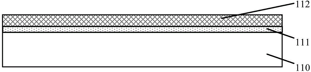
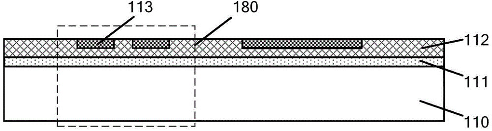
[0188] Figure 12 to Figure 15 It is a schematic cross-sectional structure diagram of the forming process of the MEMS pressure sensor according to another embodiment of the present invention.

[0189] Please refer to Figure 12 , providing a second substrate 314, the second substrate 314 includes an opposing third surface 318 and a fourth surface 319, the second substrate 314 includes a second base 310 and a pressure-sensitive pressure sensor on the second base 310 Resistive element 313, the second substrate 314 includes a pressure sensing area 380, the piezoresistive element 313 is located in the pressure sensing area 380, the piezoresistive element 313 is located in the second substrate 314 On the side of the third surface 318 , the second substrate 314 also includes a reference cell region 331 , and the piezoresistive element 313 is also located in the reference cell region 331 .

[0190] In this embodiment, the second substrate 314 further includes: a second bonding laye...


PUM


Abstract

The invention relates to an MEMS (Micro Electro Mechanical Systems) pressure sensor and a formation method thereof. The formation method comprises the following steps of providing a first substrate comprising a first surface and a second surface which are opposite, wherein the first substrate comprises at least one conducting layer, and the conducting layer is located on one side of the first surface of the first substrate; providing a second substrate comprising a third surface and a fourth surface which are opposite, wherein the second substrate comprises a second base, a piezoresistive element and a pressure sensing area, and the piezoresistive element is located in the pressure sensing area and on one side of the third surface of the second substrate; mutually fixing the first surface of the first substrate and the third surface of the second substrate; forming a cavity between the first substrate and the pressure sensing area of the second substrate; removing the second base, and forming a fifth surface opposite to the third surface of the second substrate; forming a first conductive plug penetrating to the surface of the at least one conducting layer from one side of the fifth surface of the second substrate. The performance and the reliability of the MEMS pressure sensor are improved, and the size is reduced, and the processing cost is reduced.

Description

technical field [0001] The invention relates to the technical field of semiconductor manufacturing, in particular to a MEMS pressure sensor and a forming method thereof. Background technique [0002] Micro-Electro Mechanical System (MEMS for short) is an integrated device that acquires information, processes information and performs operations. Sensors in MEMS can receive external information such as pressure, position, velocity, acceleration, magnetic field, temperature or humidity, and convert the obtained external information into electrical signals for processing in MEMS. Common microelectromechanical systems include temperature sensors, pressure sensors, and humidity sensors. [0003] For the MEMS pressure sensor, its size is smaller, and its process precision, and its manufacturing process can be compatible with the manufacturing process of integrated circuit chips, thus greatly improving the cost performance. Current MEMS pressure sensors include piezoresistive pres...

Claims


Application Information

Patent Timeline
Patent Type & Authority Applications(China)
IPC IPC(8): G01L1/22G01L1/14B81C1/00
CPCG01L9/0052B81C1/00246B81B7/008B81B2201/0264B81B2207/015B81B2207/07B81B2207/99G01L9/0073
Inventor 周文卿
Owner MEMSEN ELECTRONICS
Why Eureka
Try Eureka